Tampilkan postingan dengan label Orcad capture tutorial. Tampilkan semua postingan
Kamis, 27 Desember 2012
Senin, 12 November 2012
PSK Modulation Simulation Video Tutorial
This video tutorial shows PSK modulation simulation using Orcad Capture software. The modulator is a Ring Modulator. The Message signal is in the form of binary sequences and fed into the secondary coil of the center tapped transformer of the modulator while the carrier signal is fed into the primary winding. At the other side of the ring modulator, PSK signal is generated. This is shown in graph plot.
<math xmlns='http://www.w3.org/1998/Math/MathML'><mrow><mrow><mi mathcolor='#0000ff' color='#0000ff' fontstyle='2D Output' fontweight='normal'>s</mi><mo>⁡</mo><mfenced open='(' close=')' separators=','><mrow><mi mathcolor='#0000ff' color='#0000ff' fontstyle='2D Output' fontweight='normal'>t</mi></mrow></mfenced></mrow><mo>=</mo><mrow><mi mathcolor='#0000ff' color='#0000ff' fontstyle='2D Output' fontweight='normal'>A</mi><mo>⁢</mo><mrow><mi mathcolor='#0000ff' mathvariant='normal' color='#0000ff' fontstyle='2D Output' fontweight='normal'>cos</mi><mo>⁡</mo><mfenced open='(' close=')' separators=','><mrow><mrow><mrow><mn mathcolor='#0000ff' color='#0000ff' fontstyle='2D Output' fontweight='normal'>2</mn><mo>⁢</mo><mo>⁢</mo><mi mathcolor='#0000ff' color='#0000ff' fontstyle='2D Output' fontweight='normal'>t</mi></mrow><mo>+</mo><mfenced open='{' close='}' separators=','><mrow><mi mathcolor='#0000ff' color='#0000ff' fontstyle='2D Output' fontweight='normal'></mi></mrow></mfenced></mrow></mrow></mfenced></mrow></mrow></mrow></math>
Kamis, 01 November 2012
PSK modulation orcad capture tutorial
In this orcad capture tutorial, PSK modulation setup in orcad capture schematic, simulation and graph plot of PSK signal, binary message signal and the carrier signal is shown. A Ring Modulator is used for the modulation of the binary message signal with the high frequency carrier signal.
The PSK Modulation Schematic is shown below-
In the schematic above the carrier signal is a 10KHz sinusoid with amplitude of 10V and is applied to the primary winding of the center tapped transformer which is a part of the Ring Modulator. The message signal is a binary sequence of polar type of voltage -5V and +5V, with pulse width of 2ms and period of 4ms and rise time, fall time of 0.1us. This pulsed message signal is applied to the secondary winding of the input transformer. The four diodes(D1N4934) forms the ring of the Ring Modulator. At the other end an output center tapped transformer produces PSK signal.
The binary message signal waveform, the carrier signal waveform and the resulting PSK signal waveform is shown below-
Spectrum of PSK signal is shown below-
From the PSK frequency spectrum above we can see that most of the engery/power/amplitude is concentrated with 20KHs. The maximum amplitude is 750mV which occurs at 10KHz(the carrier signal frequency). Harmonics are present at 25KHz, 50KHz, 70KHz and so on.
The carrier signal frequency spectrum is shown below-
Binary Message Signal Frequency Spectrum is shown below-
From the graph above we can see that most of the energy/power or amplitude of the binary message is contained in the bandwidth of 0 to 5KHz.
Also ASK modulation and ASK modulation video tutorial
The PSK Modulation Schematic is shown below-
![]() |
| Fig: PSK Modulation Schematic |
The binary message signal waveform, the carrier signal waveform and the resulting PSK signal waveform is shown below-
Spectrum of PSK signal is shown below-
![]() |
| Fig: PSK signal Spectrum |
From the PSK frequency spectrum above we can see that most of the engery/power/amplitude is concentrated with 20KHs. The maximum amplitude is 750mV which occurs at 10KHz(the carrier signal frequency). Harmonics are present at 25KHz, 50KHz, 70KHz and so on.
The carrier signal frequency spectrum is shown below-
![]() |
| Fig:carrier signal spectrum |
![]() |
| Fig: Binary Message Frequency Spectrum |
From the graph above we can see that most of the energy/power or amplitude of the binary message is contained in the bandwidth of 0 to 5KHz.
Also ASK modulation and ASK modulation video tutorial
Rabu, 31 Oktober 2012
ASK modulation using Orcad Capture
ASK modulation is digital modulation technique wherein binary message signal stream is impressed onto the high frequency carrier signal for transmission over larger bandwidth channels such as air. The binary message signal stream is of unipolar type, that means that 1V represents logical 1 and 0V represents the logical 0 bit. The binary message stream turns On/Off the modulator such that the high frequency carrier signal is transmitted when modulator is switched on and during the off state nothing is transmitted.
In orcad capture a voltage controlled switch called Sbreak can be used to stimulate the behavior of the modulator. In reality a modulator is made of transistors that switches on/off in response to clock impulses supplied to it.
The schematic for simulating ASK modulation is shown in figure below-
In the schematic, the message signal labelled Message_Signal is a binary unipolar signal with V1=0V and V2=1V, TD=0s, TR=0.01us, TF=0.01us, PW=30us and PER=90us. The carrier signal labelled Carrier_Signal is a sinusoid with amplitude VAMPL=10V and frequency of 100KHz. The message binary sequence turns on/off the switch and carrier signal is transmitted as ASK signal labelled ASK_Signal. The 1k load resistance at the output simulates the resistance of the switch(modulator).
The simulation setting is shown in the figure below-
The output graph shown below shows the result of the simulation. The top graph is the binary message signal, the middle graph is the carrier signal waveform and the bottom graph is the ASK signal waveform.
Also see ASK Modulation Video Tutorial
Download ASK modulation simulation files:
http://www.filefactory.com/file/33tovaqoj98f/ASK_zip
For Phase modulation tutorial- see PSK modulation using orcad capture
In orcad capture a voltage controlled switch called Sbreak can be used to stimulate the behavior of the modulator. In reality a modulator is made of transistors that switches on/off in response to clock impulses supplied to it.
The schematic for simulating ASK modulation is shown in figure below-
![]() |
| Fig: ASK modulation schematic |
The simulation setting is shown in the figure below-
![]() |
| Fig: Simulation setting for ASK modulation |
The output graph shown below shows the result of the simulation. The top graph is the binary message signal, the middle graph is the carrier signal waveform and the bottom graph is the ASK signal waveform.
![]() |
| Fig: ASK modulation simulation output graph |
Download ASK modulation simulation files:
http://www.filefactory.com/file/33tovaqoj98f/ASK_zip
For Phase modulation tutorial- see PSK modulation using orcad capture
Rabu, 29 Agustus 2012
Creating new model in Orcad Capture
In this orcad capture tutorial it will be shown how to create a model library file(.lib) and model symbol file(.olb) for the transistor in Orcad capture which are required for simulation.
Lets say we require 2N3904 transistor in our design work. If we search this transistor we will find it under the library "Transistor" but it has no simulation model and footprint as shown below-
Now we will show how to create a simulation model for transistors like 2N3904 but any component like an IC can be added this way.
1. The first step is to download pspice model for this transistor. The pspice model for components are usually available in the manufacturer website. If the model is not available then another way to create the model is to write the pspice model in a simple text notepad by reading the datasheet of the transistor.
As an example we will show here how to create a pspice model if the pspice is not available in manufacturer website.
The 2N3904 transistor spice model is shown below-
*Model for 2N3904 NPN BJT
.model Q2N3904 NPN(Is=6.734f Xti=3 Eg=1.11 Vaf=74.03 Bf=416.4 Ne=1.259 +Ise=6.734f Ikf=66.78m Xtb=1.5 Br=.7371 Nc=2 Isc=0 Ikr=0 Rc=1 +Cjc=3.638p Mjc=.3085 Vjc=.75 Fc=.5 Cje=4.493p Mje=.2593 Vje=.75
+Tr=239.5n Tf=301.2p Itf=.4 Vtf=4 Xtf=2 Rb=10)
Now copy and paste these text into a notepad and save it with name Q2N3904 (or just 2N3904)and extension .lib, that is as Q2N3904.lib. This file is called the Model Library. Save the file in some location in your computer.
2. Now we have to create the symbol library file for the model library. To do this open the model editor as shown-
Next select "Pspice A/D" and when model editor opens select "Capture" and click done as shown-
Now go to the File> Model Import Wizard[Capture] as shown-
A new window opens that lets you import the model created earlier. Browse to the location where you previously saved "Q2N3904.lib" file. This is shown below-
Once the Q2N3904 model library (Q2N3904.lib) is imported, the destination location for the corresponding Q2N3904 symbol library will be saved in the same folder(directory) location. So leave the destination symbol library option in default. Click next.
A new window will appear that allows us to associate symbol to the model we are creating. We can choose an existing transistor symbol from the library. In this case, the symbol is matched so we don't need to search for a matching symbol.
Click Finish and the result of this operation will be shown. Notice that there is no error as shown below. Click OK to finish the model creation part.
Now both the model library file(.lib) and model symbol file(.olb) for the transistor is created.
Our transistor model not located in the default Cadence directory. Therefore, to mention the directory for the program to find the newly created model files, go to Pspice>Edit Simulation Profile option. This will bring up a window.
Select the Configuration Files tab and the Libary option on the left side. Click on browse and browse to the directory(folder) where the Q2N3904.olb file is located and select it. Then click on Add as Global or Add to Design. These process is shown in figure below-
Now the transistor is ready to go for simulation. Select the browse button in the Place Part as shown in figure below. Browse to the location of the Q2N3904.olb folder and click open.
The transistor appears in the part window and is ready to be placed onto the schematic. As shown in figure below, the pspice model and footprint icon is also visible now showing that it can be used for simulation and for PCB design.
Now the Q2N3904 transistor can be placed onto the schematic. This completes the Orcad Capture tutorial of creating a new Model required for simulation of parts in Orcad capture.
Lets say we require 2N3904 transistor in our design work. If we search this transistor we will find it under the library "Transistor" but it has no simulation model and footprint as shown below-
Now we will show how to create a simulation model for transistors like 2N3904 but any component like an IC can be added this way.
1. The first step is to download pspice model for this transistor. The pspice model for components are usually available in the manufacturer website. If the model is not available then another way to create the model is to write the pspice model in a simple text notepad by reading the datasheet of the transistor.
As an example we will show here how to create a pspice model if the pspice is not available in manufacturer website.
The 2N3904 transistor spice model is shown below-
*Model for 2N3904 NPN BJT
.model Q2N3904 NPN(Is=6.734f Xti=3 Eg=1.11 Vaf=74.03 Bf=416.4 Ne=1.259 +Ise=6.734f Ikf=66.78m Xtb=1.5 Br=.7371 Nc=2 Isc=0 Ikr=0 Rc=1 +Cjc=3.638p Mjc=.3085 Vjc=.75 Fc=.5 Cje=4.493p Mje=.2593 Vje=.75
+Tr=239.5n Tf=301.2p Itf=.4 Vtf=4 Xtf=2 Rb=10)
Now copy and paste these text into a notepad and save it with name Q2N3904 (or just 2N3904)and extension .lib, that is as Q2N3904.lib. This file is called the Model Library. Save the file in some location in your computer.
2. Now we have to create the symbol library file for the model library. To do this open the model editor as shown-
Next select "Pspice A/D" and when model editor opens select "Capture" and click done as shown-
Now go to the File> Model Import Wizard[Capture] as shown-
A new window opens that lets you import the model created earlier. Browse to the location where you previously saved "Q2N3904.lib" file. This is shown below-
Once the Q2N3904 model library (Q2N3904.lib) is imported, the destination location for the corresponding Q2N3904 symbol library will be saved in the same folder(directory) location. So leave the destination symbol library option in default. Click next.
A new window will appear that allows us to associate symbol to the model we are creating. We can choose an existing transistor symbol from the library. In this case, the symbol is matched so we don't need to search for a matching symbol.
Click Finish and the result of this operation will be shown. Notice that there is no error as shown below. Click OK to finish the model creation part.
Now both the model library file(.lib) and model symbol file(.olb) for the transistor is created.
Our transistor model not located in the default Cadence directory. Therefore, to mention the directory for the program to find the newly created model files, go to Pspice>Edit Simulation Profile option. This will bring up a window.
Select the Configuration Files tab and the Libary option on the left side. Click on browse and browse to the directory(folder) where the Q2N3904.olb file is located and select it. Then click on Add as Global or Add to Design. These process is shown in figure below-
Now the transistor is ready to go for simulation. Select the browse button in the Place Part as shown in figure below. Browse to the location of the Q2N3904.olb folder and click open.
The transistor appears in the part window and is ready to be placed onto the schematic. As shown in figure below, the pspice model and footprint icon is also visible now showing that it can be used for simulation and for PCB design.
Now the Q2N3904 transistor can be placed onto the schematic. This completes the Orcad Capture tutorial of creating a new Model required for simulation of parts in Orcad capture.
Senin, 06 Agustus 2012
AMI Bipolar Encoding Circuit design example
This tutorial shows how to design a AMI Bipolar encoding circuit and simulate it using Orcad Capture and simulate the circuit to obtain the waveform. AMI(Alternative Mark Inversion) is a bipolar encoding technique that was and is still used in older PCM modems. The reason why it is useful is because if there is any bipolar violation then it is detected at the receiver and the error can be detected. The another reason is- because AMI is a bipolar RZ(Return to Zero) scheme it does not contain any DC component and therefore can used in telephony circuit where coupling transformers are used.
Circuit Schematic for AMI Bipolar Encoder
The circuit schematic of the AMI bipolar encoding circuit is shown below:
In the circuit, NRZ unipolar signal is generated using the SIM1 part from the source library. With SIM1 part we can generate a series of binary data with some defind bit period. In this example, a 7 binary bits "1011001" each of 100us(micro second) is generated and looped for 3 times.
The 7486 XOR gate, 7408 AND gate, 7401 AND gate, the transistors Q2N3906 and Q2N3904, the J-K flip flop 74107 are found in eval library. The diode D1N750 is found in the diode library. The rest are resistors, capacitors and voltage sources that are easily found.
After connecting the components as shown in the above figure, the AMI labelled wire is where the AMI bipolar signal appears.
Simulation
Create a new simulation profiel and set the simulation time for 2ms and run it. The resulting waveform is shown below-
Each bit duration is 100microsecond(100us) or 0.1 millisecond(0.1ms). From the waveform we can see that the 1 alternatives between +3V and -3V while 0 remains at 0V.
When clicking the FFT buttom on the probe we get the frequency spectrum of this RZ bipolar waveform as shown below-
From the spectrum figure 3, we can see that the AMI bipolar encoding has no DC component and thus is suitable for transmission over telephone lines and is useful for repeaters where ac coupling is required.
Also see baseband line code analysis blog post and NRZ Unipolar and NRZ Bipolar signal generation
Circuit Schematic for AMI Bipolar Encoder
The circuit schematic of the AMI bipolar encoding circuit is shown below:
![]() |
| Fig 1: AMI Bipolar Encoding Circuit Schematic |
In the circuit, NRZ unipolar signal is generated using the SIM1 part from the source library. With SIM1 part we can generate a series of binary data with some defind bit period. In this example, a 7 binary bits "1011001" each of 100us(micro second) is generated and looped for 3 times.
The 7486 XOR gate, 7408 AND gate, 7401 AND gate, the transistors Q2N3906 and Q2N3904, the J-K flip flop 74107 are found in eval library. The diode D1N750 is found in the diode library. The rest are resistors, capacitors and voltage sources that are easily found.
After connecting the components as shown in the above figure, the AMI labelled wire is where the AMI bipolar signal appears.
Simulation
Create a new simulation profiel and set the simulation time for 2ms and run it. The resulting waveform is shown below-
![]() |
| Fig 2: AMI Bipolar Encoding Pulse Waveform |
When clicking the FFT buttom on the probe we get the frequency spectrum of this RZ bipolar waveform as shown below-
![]() |
| Fig 3: AMI Bipolar Encoding with No DC component |
Also see baseband line code analysis blog post and NRZ Unipolar and NRZ Bipolar signal generation
NRZ Unipolar and NRZ Bipolar signal generation in Orcad capture
This cadence orcad tutorial shows how to generate NRZ unipolar signal and convert the NRZ unipolar to NRZ bipolar format. Next it is verified that the NRZ unipolar signal contents DC component whereas the NRZ bipolar signal does not contain any DC component.
The circuit schematic to produce NRZ unipolar and the NRZ bipolar signal is shown below:
In the schematic the NRZ unipolar signal is generated using the STIM1 part in the source library. The signal is feed into the LF411 opamp which converts the NRZ unipolar to NRZ bipolar signal at its output. Proper biasing voltage is applied to the LF411 opamp as shown in figure.
New simulation profile with run time set to 1ms and leaving the max step size blank gives the following digital waveforms.
The upper digital waveform is the bipolar NRZ signal and the lower digital waveform is the unipolar NRZ signal.
Now taking FFT of this signal waveform we get the following respective spectrum,
The lower NRZ unipolar signal spectrum contains dc component at 0 Hz whereas the NRZ polar signal spectrum contains no dc component at 0 Hz. This is a reason why NRZ encoding is unsuitable for transmission of signal over telephone copper line.
As mentioned above the schematic and simulation was done using orcad capture. Also see the analysis of polar, bipolar, NRZ and RZ blog post.
The circuit schematic to produce NRZ unipolar and the NRZ bipolar signal is shown below:
![]() |
| Fig 1: Schematic to produce NRZ unipolar and NRZ bipolar |
New simulation profile with run time set to 1ms and leaving the max step size blank gives the following digital waveforms.
![]() |
| Fig 2: Unipolar NRZ and Bipolar NRZ waveform |
Now taking FFT of this signal waveform we get the following respective spectrum,
![]() |
| Fig 3: Spectrum of NRZ Unipolar and Bipolar |
As mentioned above the schematic and simulation was done using orcad capture. Also see the analysis of polar, bipolar, NRZ and RZ blog post.
Kamis, 02 Agustus 2012
How to generate FM signal in Orcad capture
FM signal generation is required in many circuit design analysis. Instead of creating circuit level FM generator for example using BJT or FET transistor, one often requires just the FM signal to fed into the desired designed system. FM signal in orcad capture can be generated in many ways. One of the simple way is the use the VSFFM part which can be found under the source library.
The circuit for FM wave using the VSFFM FM generator is shown below:
In this VSFMM source, we can specify the modulating signal amplitude, the frequency of the modulating signal, the frequency of the carrier signal and the frequency modulation index. In this simple example the magnitude of modulating signal is VAMP=1V, modulating signal frequency, FM=1.5kHz, carrier signal frequency, FC=10kHz.
To check the Frequency modulated wave, we simulate and get the output as shown in the figure below:
To view the FM signal spectrum, we just click the FFT ion on the probe display in the Orcad capture. This gives us the following FM signal spectrum:
The spectrum clearly shows the absence of carrier part at the 10kHz.
Finally, the power developed on the resistor due to the FM signal is shown below:
See other Cadence Orcad Video Tutorials
The circuit for FM wave using the VSFFM FM generator is shown below:
In this VSFMM source, we can specify the modulating signal amplitude, the frequency of the modulating signal, the frequency of the carrier signal and the frequency modulation index. In this simple example the magnitude of modulating signal is VAMP=1V, modulating signal frequency, FM=1.5kHz, carrier signal frequency, FC=10kHz.
To check the Frequency modulated wave, we simulate and get the output as shown in the figure below:
To view the FM signal spectrum, we just click the FFT ion on the probe display in the Orcad capture. This gives us the following FM signal spectrum:
The spectrum clearly shows the absence of carrier part at the 10kHz.
Finally, the power developed on the resistor due to the FM signal is shown below:
See other Cadence Orcad Video Tutorials
Senin, 06 Februari 2012
Designing Transistor Circuits
Designing a Transistor Circuit is first step in any electronic and electrical circuit design. A Transistor is fundamentally the most essential part in any electronic design. This is because of transistors which makes the electronic system that we see today. Any electronic system capability comes from two things- switching and amplification. This two functions are provided by transistors. For example, in analog systems, amplifiers are needed to amplify voltage, current or Power. A power amplifier driving an antenna at the front end or a power amplifier driving a loudspeakers are examples of application of transistor in analog domain. In digital domain, transistors are used as switches that makes up the various digital gates, NAND, XOR, AND, OR etc.There are two basic types of widely used transistors- BJT(Bipolar Junction Transistor) and FET(Field Effect Transistor). Each of them have prons and cons. For example, BJT have higher speed response in comparision to FET whereas FET consumes less area than BJTs.
Before designing a transistor circuit, we must know what we want to achieve with the transistor. In order words what is the application or function of the transistor in the circuit. For example, if we want to amplify voice that can be heard on a loudspeaker we can use a transistor as an power amplifier. Here the designing transistor circuit involves, knowing what the input signal(voice) voltage magnitude and frequency are, what power or voltage is required across the loudspeaker. For this it is necessary to know the resistance or impedance of the loudspeaker. Thus the initial assumption would be to know what the input and output characteristics are. Knowing this we can go to the next step for designing the transistor circuit which is selection of the transistors to fit the application. Once the transistor is chosen, the next step is the bias the transistor which is the process of maintaining a constant required output current (the collector current) as much as possible such that the amplification is invariant to temperature changes. Once we know what collector current we require we start by biasing the transistor circuit.
There are many biasing techniques for designing transistor circuits and the most popularly used in the voltage divider biasing. See the post Amplifier Design where details of how to bias a transistor is illustrated.
Circuit Schematic of Transistor Circuit Design
Below shows a schematic drawn in orcad capture in which 2N2222 low power transistor used as an audio amplifier to amplify 0.4V, 1kHz input signal.![]() |
| Fig: Designing Transistor Circuits |
Example of Designing Transistor Circuits
Suppose we have a 8ohm loudspeaker and we require 2V across it to produce 0.5W power. Then below is detailed calculation used in the circuit-Vcc=IcRc+Vc
IcRc=Vcc-Vc
IcRc=9V-2V
IcRc=7V
Rc=7V/Ic
Rc=7/150mA
Rc=47ohm
Vce at 150mA= 1V
there,
Vce=Vc-Ve
Ve=Vc-Vce
Ve=2V-1V
Ve=1V
Ie=Ic=150mA
therefore,
Re=Ve/Ie
Re=1V/150mA
Re=6.66ohm
R2~6ohm
Vb=Vbe+Ve
Vb=0.6V+1V
Vb=1.6V
R1<100*Re/10
R1<100*6.66/10
R1<66.6ohm
R1~64ohm
Vcc=V1+V2
Vcc=V1+Vb
V1=Vcc-Vb
V1=9V-1.6V
V1=7.4V
R2=R1*V2/V1
R2=65*1.6/7.4
R2=12.97ohm
R2~15ohm
The output signal waveform from simulation for frequency from 20Hz to 1kHz is shown below-
![]() |
| Fig: All Frequency waveform at the load |
Minggu, 05 Februari 2012
Class C Power Amplifier Design and Simulation
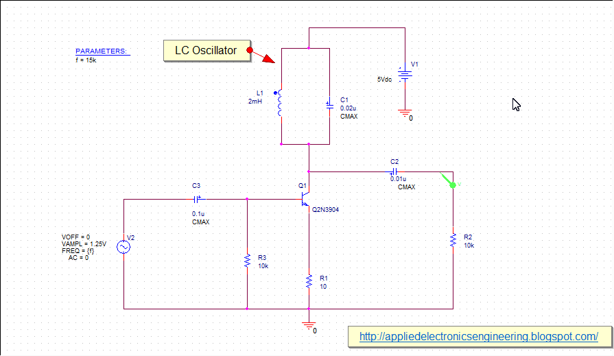
In this article Class C Power Amplifier circuit is designed stimulate using orcad capture. LC oscillator is designed to oscillate at 25kHz and then input signal frequency and amplitude is varied to get maximum output voltage.
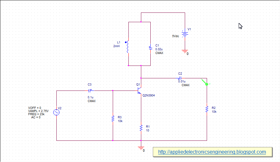
In the above schematic, an input sinusoid signal is applied which has voltage magnitude of 1.25V. The frequency(f) is varied from 15kHz to 30kHz using the parameter sweep tool available in orcad capture. This signal is fed into the class C power amplifier that is made by transistor Q2N3904, L1 and C1 which makes up the LC tuned oscillator. The resistors R3 and R1 are biasing resistors required to bias the transistors(see transistor biasing tutorial). The resistor R2 is a load resistor. The capacitors C3 and C2 are coupling capacitors that blocks dc signals and allows ac signal to pass. This circuit is run by 5V supply.
We know that the frequency of oscillation of the LC oscillator is 25kHz derived from the LC oscillator frequency formula-
\[f=\frac{1}{2\pi\sqrt{LC}}\]
Substituting 2mH for inductor and 0.02microF for capacitor gives 25kHz.
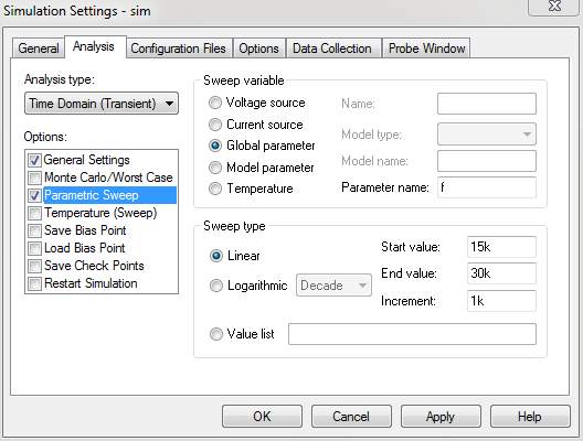
To do this we vary the frequency of the input signal using the parameter sweep tool which is located in the Special library. Then we set up the simulation setting with Transient simulation of run time of 1ms and step size is 10us. Also we set up parameter sweep with f as global parameter, linear sweep type from 15kHz to 30kHz and increment of 1kHz. This simulation setting is shown below-
We put the voltage probe tool at the output as shown in the schematic and run the simulation to get its waveform-
This waveform shows output voltage waveform for all frequency from 15kHz to 30kHz.
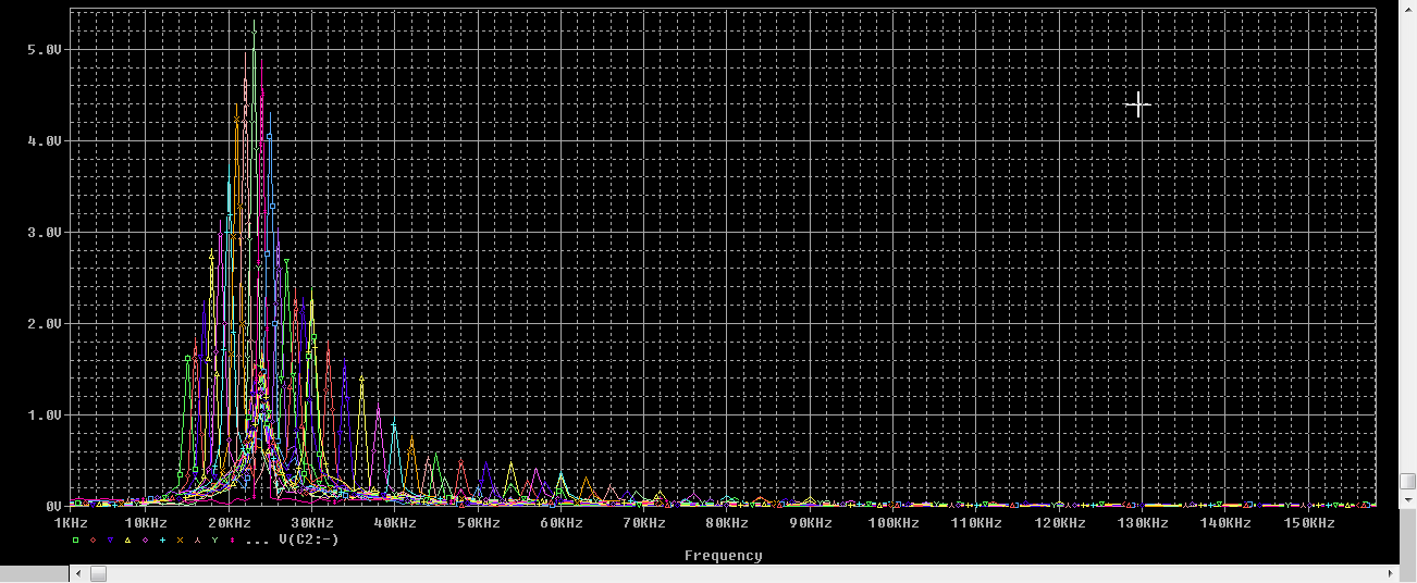
Using the FFT tool available in orcad capture we get the following FT-
To zoom in we can use the zoom area tool available in the toolbar-
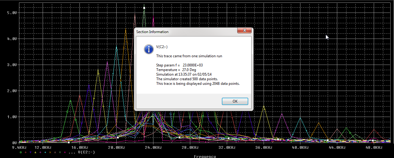
From this final FT graph we can clearly see the frequency at which the magnitude of the output signal is maximum. The green at the center has greatest peak and right clicking on it and selecting Trace Information gives us the its frequency information. This is shown below-
This information shows that the frequency of this trace is 23kHz.
We can now change the input signal frequency to this 23kHz.
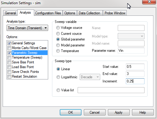
Now we can similarly vary the amplitude of the input signal using the parameter sweep tool. The amplitude is varied from 0.5V to 3V as shown-
and the voltage variation sweep settings-
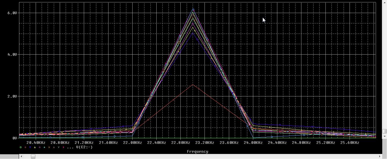
The output waveform with varying input voltage amplitude is shown below-
The Fourier Transform is shown below-
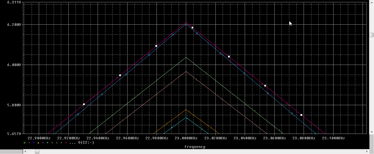
Using the Zoom Area Tool in the toolbar-
Zooming into the peak and selecting the peak signal and right clicking to get its trace information gives-
This shows that the magnitude of the input voltage at which the output voltage is maximum is 2.75V.
Changing the input voltage to 2.75V, removing the parameter sweep tool the final class C amplifier circuit is shown below-
Removing the parameter sweep in the simulation setup and running the final circuit for 2ms gives the following output signal waveform-
And the Fourier Transform gives-
This shows that the maximum output voltage is around 6V.
Class C Power Amplifier Schematic
Below is a schematic diagram of a Class C Power Amplifier.![]() |
| Fig: class C power amplifier circuit |
We know that the frequency of oscillation of the LC oscillator is 25kHz derived from the LC oscillator frequency formula-
\[f=\frac{1}{2\pi\sqrt{LC}}\]
Substituting 2mH for inductor and 0.02microF for capacitor gives 25kHz.
Class C Power Amplifier Simulation
Although we know the frequency of the oscillator we want to know what the frequency of the input signal is at which the magnitude of the output voltage is maximum given that the magnitude of the input signal voltage is 1.25V. By varying the frequency of the input signal we can get information about the frequency at which the output voltage magnitude is maximum.To do this we vary the frequency of the input signal using the parameter sweep tool which is located in the Special library. Then we set up the simulation setting with Transient simulation of run time of 1ms and step size is 10us. Also we set up parameter sweep with f as global parameter, linear sweep type from 15kHz to 30kHz and increment of 1kHz. This simulation setting is shown below-
![]() |
| Fig: Simulation setting parametric sweep |
![]() |
| Fig: Output Voltage waveforms at different input frequencies |
Using the FFT tool available in orcad capture we get the following FT-
![]() |
| Fig: Output signal waveform Fourier transform |
To zoom in we can use the zoom area tool available in the toolbar-
![]() |
| Fig: Fourier transform of Output signal waveform |
![]() |
| Fig: Fourier transform of Output signal waveform |
![]() |
| Fig: Trace Information from Fourier Transform |
We can now change the input signal frequency to this 23kHz.
Now we can similarly vary the amplitude of the input signal using the parameter sweep tool. The amplitude is varied from 0.5V to 3V as shown-
![]() |
| Fig: Class C Power Amplifier circuit with Voltage Parameter Sweep |
![]() |
| Fig: Simulation setting for voltage parameter sweep |
![]() |
| Fig: Output Voltage waveform with voltage parametric sweep |
![]() |
| Fig: Fourier Transform of output voltage |
![]() |
| Fig: Zoomed Fourier Transform of output voltage |
![]() |
| Fig: Zoomed Fourier Transform of output voltage |
![]() |
| Fig: Zoomed Fourier Transform of output voltage |
![]() |
| Fig: Output Voltage trace information |
Changing the input voltage to 2.75V, removing the parameter sweep tool the final class C amplifier circuit is shown below-
![]() |
| Fig: Final Class C Power Amplifier |
Removing the parameter sweep in the simulation setup and running the final circuit for 2ms gives the following output signal waveform-
![]() |
| Fig: Final Output voltage waveform |
![]() |
| Fig: Final Output voltage waveform |
Langganan:
Postingan (Atom)