Kamis, 27 Desember 2012
Minggu, 16 Desember 2012
D Flip Flop realization and simulation using Xilinx, Isim and Modelsim
The video below shows D Flip Flop realization in verilog HDL and simulation using Xilinx and Modelsim. First D Flip Flop is constructed in Xilinx, then it's stimulus is created also in Xilinx and then simlated using Isim and Modelsim.
Below is the video, code and some screenshots of the D flip flop schematic-
Video-
Schematics-
Verilog Codes:
A. D Flip Flop Verilog HDL code:
------------------------------------------------------------------
// D Flip Flop
module dff(
input D,
output reg Q,
output reg Qn,
input clk,
input rst
);
always @(posedge clk or negedge rst)
begin
if(rst == 1'b0)
begin
Q <= 0;
Qn <= 1;
end
else
begin
Q <= D;
Qn <= !D;
end
end
endmodule
--------------------------------------------------------------------
B. Test Module for D Flip Flop
------------------------------------------------------------------------
// Test Bench for D Flip Flop
`timescale 1ns / 10ps
module dff_test;
//Time Parameter
localparam T = 20; //20ns
// Inputs
reg D_t;
reg clk_t;
reg rst_t;
// Outputs
wire Q_t;
wire Qn_t;
// Instantiate the Unit Under Test (UUT)
dff uut (
.D(D_t),
.Q(Q_t),
.Qn(Qn_t),
.clk(clk_t),
.rst(rst_t)
);
----------------------------------------------------------------
Below is the video, code and some screenshots of the D flip flop schematic-
Video-
Schematics-
 |
| Fig: D Flip Flop |
 |
| Fig: A closer look of D Flip Flop |
A. D Flip Flop Verilog HDL code:
------------------------------------------------------------------
// D Flip Flop
module dff(
input D,
output reg Q,
output reg Qn,
input clk,
input rst
);
always @(posedge clk or negedge rst)
begin
if(rst == 1'b0)
begin
Q <= 0;
Qn <= 1;
end
else
begin
Q <= D;
Qn <= !D;
end
end
endmodule
--------------------------------------------------------------------
B. Test Module for D Flip Flop
------------------------------------------------------------------------
// Test Bench for D Flip Flop
`timescale 1ns / 10ps
module dff_test;
//Time Parameter
localparam T = 20; //20ns
// Inputs
reg D_t;
reg clk_t;
reg rst_t;
// Outputs
wire Q_t;
wire Qn_t;
// Instantiate the Unit Under Test (UUT)
dff uut (
.D(D_t),
.Q(Q_t),
.Qn(Qn_t),
.clk(clk_t),
.rst(rst_t)
);
----------------------------------------------------------------
Jumat, 14 Desember 2012
Comsol Multiphysics Tutorial on Helmholtz Equation
This short video tutorial show how to use Helmholtz equation in Comsol Multiphysics.
Kamis, 13 Desember 2012
Comsol Multiphysics Tutorial: Setting up boundary
This is a simple quick video on setting up boundary condition and mesh in Comsol Multiphysics. In this exercise a simple rectangular geometry is created and mesh are defined.
Multiplexer Design and Simulation using Xilinx and Modelsim Video Tutorial
The following quick video tutorial shows 4x1 Multiplexer design and simulation using Xilinx and Modelsim. The HDL language used in Verilog. Multiplexers are essential combinational circuit elements that are required and used in larger FPGA design. First 4x1 Mulitplexer verilog code is constructed then the test bench is created in Xilinx ISE and finally simulated in Modelsim 10.1c to verify it's correctness.
Watch the video-
For more visit FPGA design tutorials
Watch the video-
For more visit FPGA design tutorials
Rabu, 12 Desember 2012
Modelsim logic gate video tutorial
This is a quick video tutorial on how to use Modelsim for logic gate design and verification. An AND gate is constructed with verilog HDL and a testbench is also created to test it's logic. We start by creating a project in Modelsim, then create an AND gate and then the testbench. Finally operation of the gate is checked through simulation.
Watch the video below-
For more visit FPGA design tutorials
Watch the video below-
For more visit FPGA design tutorials
AND Gate verification using Xilinx and Modelsim
This quick video tutorial shows how to verify AND gate logic using Xilinx and Modelsim. Xilinx v13 and modelsim 10.1c has been used here. First a new project is created in xilinx, verilog code for AND gate is created and then verilog code for test bench is created. The code syntax is checked for correctness and then simulated using Modelsim simulator. The output corresponding to the four logic combination input, that is, 00, 01, 10 and 11 is checked.
watch the following video-
For more visit FPGA design tutorials
watch the following video-
For more visit FPGA design tutorials
Selasa, 04 Desember 2012
Convolutional Encoder FPGA Design
This is a tutorial of FPGA design of convolutional encoder in Xilinx ISE. The convolutional codes are channel codes used in wireless communication such as space communication and broadcasting applications. It is a linear code but unlike block codes in which the inputs are grouped into blocks, in covolutional encoding the input stream are encoded sequentially. Another difference is that the convolutional encoder has memory whereas block encoder does not.
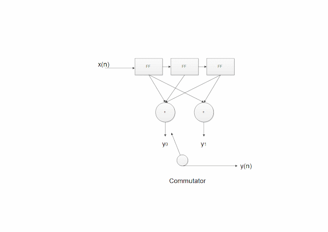
The following diagram shows the concept involved in the synthesis of encoder. The input binary signal x(n) enters the shift register at each clock frequency. At the output convolutionally encoded y(n) is produced also at the sampling frequency.
The verilog code for this convolutional encoder is shown below-
-------------------------------------------------------------------------------------------------------------
module encode_src(x,y,clk,rst);
input [3:0]x; //4-bit input data
output [1:0]y; //2-bit output data
input clk; //clock
input rst; //reset
reg [1:0]y;
reg [3:0]ff0;
reg ff1,ff2;
always@(posedge clk, posedge rst)
begin
if(rst)
begin
y <= 2'b0;
ff1 <= 1'b0;
ff2 <= 1'b0;
ff0 <= x;
end
else
begin
ff1 <= ff0[0];
ff2 <= ff1;
y[0] <= (ff0[0]^ff2);
y[1] <= ff0[0]^ff1^ff2;
ff0 <= ff0 >>1;
end
end
endmodule-------------------------------------------------------------------------------------------------------------------
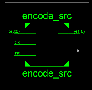
In the code x and y are the input and output. The input x is a 4 bit sequence and the output is a 2 bit sequence. clk and rst are clock and reset. The ff0, ff1 and ff2 are flip-flops. Within the always block the if-else procedural statement is applied such that first the reset(rst) is checked. If it is ON then output y, the flip-flop 1 and 2 are cleared and the input first bit is entered into the flip-flop 0. If it reset is not set then the first input entry is shifted into ff1, the content of ff1 into ff2, output y(0) and y(1) are calculated as y(0)= x(n)+x(n-2) and y(1)=x(n)+x(n-1)+x(n-2).
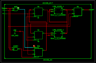
The corresponding Xilinx generated block diagram is shown below-
The following diagram shows the concept involved in the synthesis of encoder. The input binary signal x(n) enters the shift register at each clock frequency. At the output convolutionally encoded y(n) is produced also at the sampling frequency.
 |
| Figure: Convolutional Encoder |
The verilog code for this convolutional encoder is shown below-
-------------------------------------------------------------------------------------------------------------
module encode_src(x,y,clk,rst);
input [3:0]x; //4-bit input data
output [1:0]y; //2-bit output data
input clk; //clock
input rst; //reset
reg [1:0]y;
reg [3:0]ff0;
reg ff1,ff2;
always@(posedge clk, posedge rst)
begin
if(rst)
begin
y <= 2'b0;
ff1 <= 1'b0;
ff2 <= 1'b0;
ff0 <= x;
end
else
begin
ff1 <= ff0[0];
ff2 <= ff1;
y[0] <= (ff0[0]^ff2);
y[1] <= ff0[0]^ff1^ff2;
ff0 <= ff0 >>1;
end
end
endmodule-------------------------------------------------------------------------------------------------------------------
In the code x and y are the input and output. The input x is a 4 bit sequence and the output is a 2 bit sequence. clk and rst are clock and reset. The ff0, ff1 and ff2 are flip-flops. Within the always block the if-else procedural statement is applied such that first the reset(rst) is checked. If it is ON then output y, the flip-flop 1 and 2 are cleared and the input first bit is entered into the flip-flop 0. If it reset is not set then the first input entry is shifted into ff1, the content of ff1 into ff2, output y(0) and y(1) are calculated as y(0)= x(n)+x(n-2) and y(1)=x(n)+x(n-1)+x(n-2).
The corresponding Xilinx generated block diagram is shown below-
Langganan:
Komentar (Atom)


