This is a tutorial series on microstrip patch antenna design with inset feed in CST microwave. The antenna will be designed to work in 2.4GHz ISM band used in WiFi devices.
The overall design steps for designing the patch antenna in CST microwave studio involves-
1. Calculation of the dimension of the patch antenna, substrate, ground plane, effective dielectric constant, impedance etc.
2. Inputting the parameter obtained into the CST microwave studio, draw the substrate,, ground plane, patch antenna, gap between the patch and microstrip feed and microstrip feed.
3. Simulation and Optimization
The patch antenna picture that will be designed is shown below-
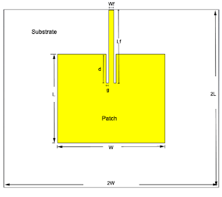 Because it is a lengthy process, each step is described in different blog post. The first step which involves the calculation is described in this post. Readers can skip to-
2nd Part- Design of Microstrip Patch Antenna in CST Microwave Studio
3rd Part- Inset Fed Patch Antenna Simulation and Result
Design Specification:
Suppose we want to design the patch antenna that resonates at 2.45GHz on a RT/Duroid 5870 substrate. The RT/Duroid substrate has a dielectric constant of 2.33 and a thickness (or height) of 0.787mm.
The first step is determine the length and width of the patch antenna. These can be determined using the following equations-
For Width,
\(\begin{equation}W=\frac{c}{2f_r}\sqrt{\frac{ 2}{\epsilon_r+1}} \end{equation}\) ........(1)
where,
c is the speed of light, \(\begin{equation}c=3\times10^{8}m/sec \end{equation}\)
fr is the resonant frequency, \(\begin{equation}f_r=2.4835GHz \end{equation}\)
\(\begin{equation}\epsilon_r\end{equation}\) is the dielectric constant of RT/Duroid substrate, \(\begin{equation}\epsilon_r=2.33\end{equation}\)
substituting the values gives us, W = 47.44mm
For Length,
first determine the effective dielectric constant,
\(\begin{equation}\epsilon_{eff}=\frac{\epsilon_r+1}{2}+\frac{\epsilon_r-1}{2}\frac{1}{\sqrt{1+\frac{12h}{W}}} \end{equation}\) ............(2)
\(\begin{equation}\epsilon_{eff}=2.272 \end{equation}\)
then find the extended incremental length,
\(\begin{equation}\triangle{L}=0.412*h\frac{(\epsilon_{eff}+0.3)(\frac{W}{h}+0.264)}{(\epsilon_{eff}+0.258)(\frac{W}{h}+0.8)} \end{equation}\) ............(3)
using the values we find,
\(\begin{equation}\triangle{L}=1mm \end{equation}\)
Now the length of the patch antenna can be obtained using the equation below,
\(\begin{equation} L=\frac{c}{2f_r\sqrt{\epsilon_r}}- 2*\triangle{L}\end{equation}\) ........(4)
Substituting the known values we obtain the length of the patch antenna as, L = 39.618mm
The next step is to determine the Inset feed point.
What is the inset feed point? It is a point located inside the patch where the impedance of the feed microstrip and the patch antenna is matched or becomes equal and thus least amount of energy is reflected back to the microstrip and most of the energy is radiated from the antenna.
Let the distance of the inset feed point be d from one of the edge of the patch antenna. Let us use a 50ohm microstrip feed and find the inset point where this 50ohm will match the input impedance of the patch antenna.
The equation to find out the value of d is,
\(\begin{equation} R_{f,in}(d)=R_{p,in}(0)*cos^2(\frac{\pi*d}{L})\end{equation}\) ........(6)
where,
\(\begin{equation} R_{p,in}(0)=\frac{1}{2(G_1\pm G_{12})}\end{equation}\) ........(7)
here \(\begin{equation}G_1\end{equation}\) is the conductance at the entry slot and \(\begin{equation}G_{12}\end{equation}\) is the mutual conductance between the entry and second slot.
Using approximation,
\(\begin{equation} R_{p,in}(0)=\frac{1}{2G_1}\end{equation}\) ........(8)
The value of \(\begin{equation} G_1\end{equation}\) is given by,
\(\begin{equation} G_1=\frac{cos(k*W)+k*W*S_i(k*W)+\frac{Sin(k*W)}{k*W}-2}{120*\pi^2}\end{equation}\) ...............(9)
where, k is the wave vector, \(\begin{equation}k=\frac{2\pi}{\lambda}=51.98m^{-1}\end{equation}\)
Substituting the value of W=46.8mm(0.0468m) and k=51.98 per m in equation (9), we obtain \(\begin{equation} G_1=2.855*10^{-3}S \end{equation}\)
Now, using equation (8) we obtain,
\(\begin{equation} R_{p,in}(0)=175ohm\end{equation}\)
Substituting the values of \(\begin{equation} R_{p,in}(0),R_{f,in}(d)=50ohm\end{equation}\) obtained above in equation (6) and solving for d we get,
\(\begin{equation}d=\frac{L}{\pi}\cos^{-1}(\sqrt{\frac{R_{f,in}(d)}{R_{p,in}(0)}})\end{equation}\)
d=12.697 mm
Now we have to calculate the width of the microstrip feed line with impedance of 50ohm. The width of the microstrip line can be found out using microstrip line calculator such as ADS LineCalc or using the following formula-
\(\begin{equation}Z_f=\frac{120\pi}{\sqrt{\epsilon_{eff}}[\frac{W_f}{h}+1.393+0.667*ln(\frac{W_f}{h}+1.444)]}\end{equation}\) ............(5)
Using the ADS LineCalc the width of microstrip feed \(\begin{equation}W_f\end{equation}\) and length were obtained as below-
\(\begin{equation}W_f=2.291mm\end{equation}\) and \(\begin{equation}L_f=31.949mm\end{equation}\)
We have calculated all the required dimension for the microstrip patch antenna design.
Now continue reading Design of Microstrip antenna in CST Microwave Studio
The overall design steps for designing the patch antenna in CST microwave studio involves-
1. Calculation of the dimension of the patch antenna, substrate, ground plane, effective dielectric constant, impedance etc.
2. Inputting the parameter obtained into the CST microwave studio, draw the substrate,, ground plane, patch antenna, gap between the patch and microstrip feed and microstrip feed.
3. Simulation and Optimization
The patch antenna picture that will be designed is shown below-

2nd Part- Design of Microstrip Patch Antenna in CST Microwave Studio
3rd Part- Inset Fed Patch Antenna Simulation and Result
Design Specification:
Suppose we want to design the patch antenna that resonates at 2.45GHz on a RT/Duroid 5870 substrate. The RT/Duroid substrate has a dielectric constant of 2.33 and a thickness (or height) of 0.787mm.
The first step is determine the length and width of the patch antenna. These can be determined using the following equations-
For Width,
\(\begin{equation}W=\frac{c}{2f_r}\sqrt{\frac{ 2}{\epsilon_r+1}} \end{equation}\) ........(1)
where,
c is the speed of light, \(\begin{equation}c=3\times10^{8}m/sec \end{equation}\)
fr is the resonant frequency, \(\begin{equation}f_r=2.4835GHz \end{equation}\)
\(\begin{equation}\epsilon_r\end{equation}\) is the dielectric constant of RT/Duroid substrate, \(\begin{equation}\epsilon_r=2.33\end{equation}\)
substituting the values gives us, W = 47.44mm
For Length,
first determine the effective dielectric constant,
\(\begin{equation}\epsilon_{eff}=\frac{\epsilon_r+1}{2}+\frac{\epsilon_r-1}{2}\frac{1}{\sqrt{1+\frac{12h}{W}}} \end{equation}\) ............(2)
\(\begin{equation}\epsilon_{eff}=2.272 \end{equation}\)
then find the extended incremental length,
\(\begin{equation}\triangle{L}=0.412*h\frac{(\epsilon_{eff}+0.3)(\frac{W}{h}+0.264)}{(\epsilon_{eff}+0.258)(\frac{W}{h}+0.8)} \end{equation}\) ............(3)
using the values we find,
\(\begin{equation}\triangle{L}=1mm \end{equation}\)
Now the length of the patch antenna can be obtained using the equation below,
\(\begin{equation} L=\frac{c}{2f_r\sqrt{\epsilon_r}}- 2*\triangle{L}\end{equation}\) ........(4)
Substituting the known values we obtain the length of the patch antenna as, L = 39.618mm
The next step is to determine the Inset feed point.
What is the inset feed point? It is a point located inside the patch where the impedance of the feed microstrip and the patch antenna is matched or becomes equal and thus least amount of energy is reflected back to the microstrip and most of the energy is radiated from the antenna.
Let the distance of the inset feed point be d from one of the edge of the patch antenna. Let us use a 50ohm microstrip feed and find the inset point where this 50ohm will match the input impedance of the patch antenna.
The equation to find out the value of d is,
\(\begin{equation} R_{f,in}(d)=R_{p,in}(0)*cos^2(\frac{\pi*d}{L})\end{equation}\) ........(6)
where,
\(\begin{equation} R_{p,in}(0)=\frac{1}{2(G_1\pm G_{12})}\end{equation}\) ........(7)
here \(\begin{equation}G_1\end{equation}\) is the conductance at the entry slot and \(\begin{equation}G_{12}\end{equation}\) is the mutual conductance between the entry and second slot.
Using approximation,
\(\begin{equation} R_{p,in}(0)=\frac{1}{2G_1}\end{equation}\) ........(8)
The value of \(\begin{equation} G_1\end{equation}\) is given by,
\(\begin{equation} G_1=\frac{cos(k*W)+k*W*S_i(k*W)+\frac{Sin(k*W)}{k*W}-2}{120*\pi^2}\end{equation}\) ...............(9)
where, k is the wave vector, \(\begin{equation}k=\frac{2\pi}{\lambda}=51.98m^{-1}\end{equation}\)
Substituting the value of W=46.8mm(0.0468m) and k=51.98 per m in equation (9), we obtain \(\begin{equation} G_1=2.855*10^{-3}S \end{equation}\)
Now, using equation (8) we obtain,
\(\begin{equation} R_{p,in}(0)=175ohm\end{equation}\)
Substituting the values of \(\begin{equation} R_{p,in}(0),R_{f,in}(d)=50ohm\end{equation}\) obtained above in equation (6) and solving for d we get,
\(\begin{equation}d=\frac{L}{\pi}\cos^{-1}(\sqrt{\frac{R_{f,in}(d)}{R_{p,in}(0)}})\end{equation}\)
d=12.697 mm
Now we have to calculate the width of the microstrip feed line with impedance of 50ohm. The width of the microstrip line can be found out using microstrip line calculator such as ADS LineCalc or using the following formula-
\(\begin{equation}Z_f=\frac{120\pi}{\sqrt{\epsilon_{eff}}[\frac{W_f}{h}+1.393+0.667*ln(\frac{W_f}{h}+1.444)]}\end{equation}\) ............(5)
Using the ADS LineCalc the width of microstrip feed \(\begin{equation}W_f\end{equation}\) and length were obtained as below-
\(\begin{equation}W_f=2.291mm\end{equation}\) and \(\begin{equation}L_f=31.949mm\end{equation}\)
We have calculated all the required dimension for the microstrip patch antenna design.
Now continue reading Design of Microstrip antenna in CST Microwave Studio


