In this orcad capture tutorial, PSK modulation setup in orcad capture schematic, simulation and graph plot of PSK signal, binary message signal and the carrier signal is shown. A Ring Modulator is used for the modulation of the binary message signal with the high frequency carrier signal.
The PSK Modulation Schematic is shown below-
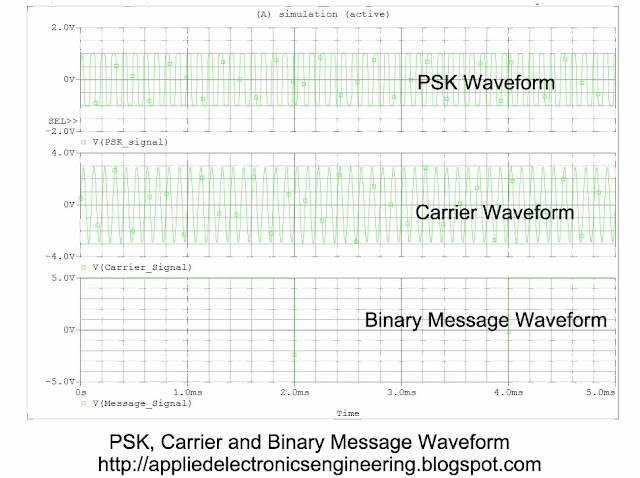
In the schematic above the carrier signal is a 10KHz sinusoid with amplitude of 10V and is applied to the primary winding of the center tapped transformer which is a part of the Ring Modulator. The message signal is a binary sequence of polar type of voltage -5V and +5V, with pulse width of 2ms and period of 4ms and rise time, fall time of 0.1us. This pulsed message signal is applied to the secondary winding of the input transformer. The four diodes(D1N4934) forms the ring of the Ring Modulator. At the other end an output center tapped transformer produces PSK signal.
The binary message signal waveform, the carrier signal waveform and the resulting PSK signal waveform is shown below-
Spectrum of PSK signal is shown below-
From the PSK frequency spectrum above we can see that most of the engery/power/amplitude is concentrated with 20KHs. The maximum amplitude is 750mV which occurs at 10KHz(the carrier signal frequency). Harmonics are present at 25KHz, 50KHz, 70KHz and so on.
The carrier signal frequency spectrum is shown below-
Binary Message Signal Frequency Spectrum is shown below-
From the graph above we can see that most of the energy/power or amplitude of the binary message is contained in the bandwidth of 0 to 5KHz.
Also ASK modulation and ASK modulation video tutorial
The PSK Modulation Schematic is shown below-
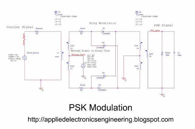 |
| Fig: PSK Modulation Schematic |
The binary message signal waveform, the carrier signal waveform and the resulting PSK signal waveform is shown below-
Spectrum of PSK signal is shown below-
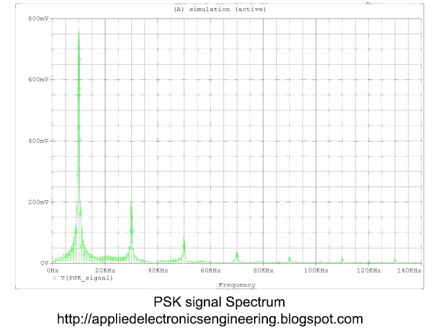 |
| Fig: PSK signal Spectrum |
From the PSK frequency spectrum above we can see that most of the engery/power/amplitude is concentrated with 20KHs. The maximum amplitude is 750mV which occurs at 10KHz(the carrier signal frequency). Harmonics are present at 25KHz, 50KHz, 70KHz and so on.
The carrier signal frequency spectrum is shown below-
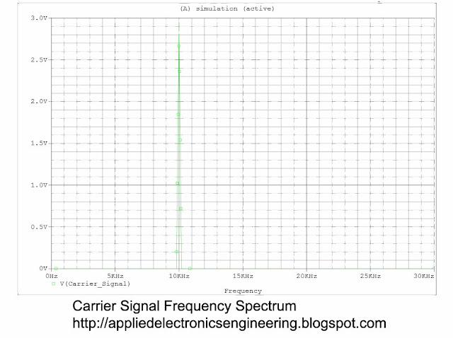 |
| Fig:carrier signal spectrum |
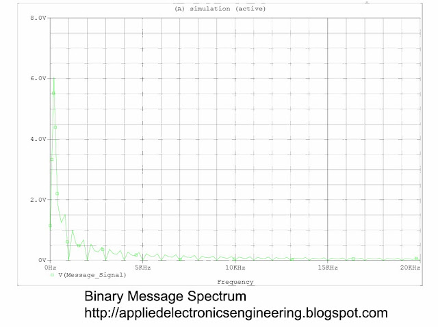 |
| Fig: Binary Message Frequency Spectrum |
From the graph above we can see that most of the energy/power or amplitude of the binary message is contained in the bandwidth of 0 to 5KHz.
Also ASK modulation and ASK modulation video tutorial
Tidak ada komentar:
Posting Komentar