This tutorial shows how to add 3D PCB step model in Altium Designer.
For more PCB design tutorials visit- Altium Designer Tutorials
Suppose you have a component which has a schematic symbol and footprint but does not have a 3D model. As an example, consider the case where we have the Atmel's ATmega8-16AC which is a 8bit microcontroller. This microcontroller chip has a schematic symbol and footprint as shown-

Now if the schematic symbol is double clicked it brings up a new window showing the properties of the component. There under model you can see what other files are attached to it. Here it shows that footprint is available to it but not the 3D model.
Select the footprint and click edit. This will bring up the footprint information. This is shown below-

Now we have attach a 3D model to the footprint. To do so first we require the 3D model for this chip. To get the 3D model we can either make a new one or download an existing one from sites like 3Dcontentcentral.com.
Here we will download the 3D model of this chip from the 3Dcontentcentral.com and attach to the footprint.
To do so, follow the steps.
First go the 3Dcontentcentral.com and download the 3D model step file from the website. For this make a search and you will be shown the available model if the site has one. This is shown below-

Once the component is found, go to the download section, select the Format as STEP(*,step), and version as AP214 as shown in the figure above. Click the download button and download it to a suitable folder in your hard drive.
Now to attach this 3D model step file, we have to open the footprint of the ATmega8-16AC chip and attach the 3D step file there. To find the library that contains the ATmega8-16AC chip make a library search. Here in this case, the footprint and schematic symbol of the ATmega8-16AC chip was inside an integrated library called Atmel Microcontroller 8-Bit AVR. This is shown below-

To get the footprint only, open the integrated library and altium designer will ask whether to extract the integrated library. Select Extract the integrated library. It will be extracted in the same folder containing the integrated library, see above picture.
Once the integrated library is extracted, the schematic library and the PCB library(footprint library) will be visible in the project panel as shown below-

Now select the Atmel Microcontroller 8-Bit AVR.SchLib and then click on the SCH Library tab at the bottom of the project panel and select the ATmega8-16AC. This is shown below-

This is the schematic component/part to which the 3D model will be attached.
Now having noted footprint used for this schematic part, we continue to select its corresponding footprint. To do this go back to the project panel, select the Atmel Microcontroller 8-Bit AVR.PcbLib and click on the PCB Library tab at the bottom of the panel then select the 32A_M footprint from the library as shown-

Now go to 3D view by clicking on key 3 on the keyboard. This brings up the 3D view as shown-

In altium designer, sometimes 3D view will not show. This is because the 3D view is not enabled. In such case then while in the 3D mode, press key "L" and select "Yes" in the Show simple 3D bodies as shown below-

Now go to Place menu and select 3D body as shown-

This bring up a dialog box that allows us to attach the 3D step model (downloaded earlier). In the dialog that appears select the Generic STEP Model, and click on Embed Step Model. Browse to the location and select the step model file that you had downloaded earlier(or the one you want to attach). This process is shown below-

Once the step model is opened the 3D editor window will have the 3D step model added as shown below-
 Use the Shift+right mouse button to rotate the 3D models and Ctrl+right mouse button to zoom in/out.

In order to align the two 3D bodies, go to View>Workspace Panels>PCB>PCBLIB Inspector as shown-

Then select the step model 3D body that was added and information about the body will appear in the PCBLIB Inspector panel as shown-

Now we can perform rotation of the 3D body by providing model rotation angle. Here in this case, entering 90 degree rotation angle in the model rotation X will rotate the 3D body as shown-

Depending upon the orientation you should enter the appropriate rotation angle.
To align and have a top view, go to View>Zero Rotation as shown-

Press key 2 to switch to 2D view and to see the center of the component.

Switch back to 3D view and rotate the body upside down as shown-

To align the two component together we need the center of the 3D body(step model). To mark the center of the 3D body (step model) proceed as follows. Select Tool>3D Body Placement>Add Snap Points from Vertices as shown.

Go to the one of the bottom edge of the chip and click once on the edge as shown below-

Now press Spacebar key to enter the midpoint mode. Click then again once on the same vertex and go to the opposite end vertex and click on that vertex.

Now there is a center snap point at the center of the chip.

Switch to 2D view now-

Drag the 2D part of the model with white cross center to the center of the 2D footprint so that their center align as shown-

Switch to 3D view again, the top view is shown below-

The orthogonal top view-

Go to Tool>Remove Snap Points and click on the snap points to remove the snap points.

Double click on the 3D body. This will bring up the extruded 3D body and the step model 3D body information and editing window.

Double click on the extruded 3D option, and standoff height as 0.9mm and standoff height as 0.2mm as shown below-

Double click on the generic step model editor and set the standoff height as 0.6mm as shown-

Now the final 3D model should look like the followings-


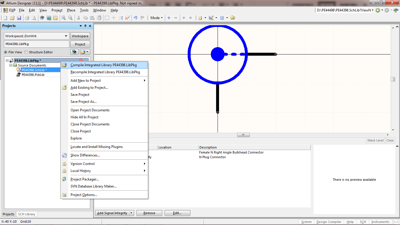
Now compile and save the integrated library project in some suitable folder.
Now bring up a new schematic sheet and place the ATMega8-16 component onto the sheet.

Now double click the component and it will bring up its properties window. Select the 32A_M footprint and you can see that the 3D step model has been added as shown below-

This completes the tutorial on adding 3D step model of ATmega8-16 in altium designer.
For more tutorials see Altium Designer Tutorials
For more PCB design tutorials visit- Altium Designer Tutorials
Suppose you have a component which has a schematic symbol and footprint but does not have a 3D model. As an example, consider the case where we have the Atmel's ATmega8-16AC which is a 8bit microcontroller. This microcontroller chip has a schematic symbol and footprint as shown-

Now if the schematic symbol is double clicked it brings up a new window showing the properties of the component. There under model you can see what other files are attached to it. Here it shows that footprint is available to it but not the 3D model.
Select the footprint and click edit. This will bring up the footprint information. This is shown below-

Now we have attach a 3D model to the footprint. To do so first we require the 3D model for this chip. To get the 3D model we can either make a new one or download an existing one from sites like 3Dcontentcentral.com.
Here we will download the 3D model of this chip from the 3Dcontentcentral.com and attach to the footprint.
To do so, follow the steps.
First go the 3Dcontentcentral.com and download the 3D model step file from the website. For this make a search and you will be shown the available model if the site has one. This is shown below-

Once the component is found, go to the download section, select the Format as STEP(*,step), and version as AP214 as shown in the figure above. Click the download button and download it to a suitable folder in your hard drive.
Now to attach this 3D model step file, we have to open the footprint of the ATmega8-16AC chip and attach the 3D step file there. To find the library that contains the ATmega8-16AC chip make a library search. Here in this case, the footprint and schematic symbol of the ATmega8-16AC chip was inside an integrated library called Atmel Microcontroller 8-Bit AVR. This is shown below-

To get the footprint only, open the integrated library and altium designer will ask whether to extract the integrated library. Select Extract the integrated library. It will be extracted in the same folder containing the integrated library, see above picture.
Once the integrated library is extracted, the schematic library and the PCB library(footprint library) will be visible in the project panel as shown below-

Now select the Atmel Microcontroller 8-Bit AVR.SchLib and then click on the SCH Library tab at the bottom of the project panel and select the ATmega8-16AC. This is shown below-

This is the schematic component/part to which the 3D model will be attached.
Now having noted footprint used for this schematic part, we continue to select its corresponding footprint. To do this go back to the project panel, select the Atmel Microcontroller 8-Bit AVR.PcbLib and click on the PCB Library tab at the bottom of the panel then select the 32A_M footprint from the library as shown-

Now go to 3D view by clicking on key 3 on the keyboard. This brings up the 3D view as shown-

In altium designer, sometimes 3D view will not show. This is because the 3D view is not enabled. In such case then while in the 3D mode, press key "L" and select "Yes" in the Show simple 3D bodies as shown below-

Now go to Place menu and select 3D body as shown-

This bring up a dialog box that allows us to attach the 3D step model (downloaded earlier). In the dialog that appears select the Generic STEP Model, and click on Embed Step Model. Browse to the location and select the step model file that you had downloaded earlier(or the one you want to attach). This process is shown below-

Once the step model is opened the 3D editor window will have the 3D step model added as shown below-


In order to align the two 3D bodies, go to View>Workspace Panels>PCB>PCBLIB Inspector as shown-

Then select the step model 3D body that was added and information about the body will appear in the PCBLIB Inspector panel as shown-

Now we can perform rotation of the 3D body by providing model rotation angle. Here in this case, entering 90 degree rotation angle in the model rotation X will rotate the 3D body as shown-

Depending upon the orientation you should enter the appropriate rotation angle.
To align and have a top view, go to View>Zero Rotation as shown-

Press key 2 to switch to 2D view and to see the center of the component.

Switch back to 3D view and rotate the body upside down as shown-

To align the two component together we need the center of the 3D body(step model). To mark the center of the 3D body (step model) proceed as follows. Select Tool>3D Body Placement>Add Snap Points from Vertices as shown.

Go to the one of the bottom edge of the chip and click once on the edge as shown below-

Now press Spacebar key to enter the midpoint mode. Click then again once on the same vertex and go to the opposite end vertex and click on that vertex.

Now there is a center snap point at the center of the chip.

Switch to 2D view now-

Drag the 2D part of the model with white cross center to the center of the 2D footprint so that their center align as shown-

Switch to 3D view again, the top view is shown below-

The orthogonal top view-

Go to Tool>Remove Snap Points and click on the snap points to remove the snap points.

Double click on the 3D body. This will bring up the extruded 3D body and the step model 3D body information and editing window.

Double click on the extruded 3D option, and standoff height as 0.9mm and standoff height as 0.2mm as shown below-

Double click on the generic step model editor and set the standoff height as 0.6mm as shown-

Now the final 3D model should look like the followings-


Now compile and save the integrated library project in some suitable folder.
Now bring up a new schematic sheet and place the ATMega8-16 component onto the sheet.

Now double click the component and it will bring up its properties window. Select the 32A_M footprint and you can see that the 3D step model has been added as shown below-

This completes the tutorial on adding 3D step model of ATmega8-16 in altium designer.
For more tutorials see Altium Designer Tutorials