Rabu, 12 September 2012

PCB Component placement strategy using Proteus 8

The PCB layout editor of Proteus Professional 8 has many very helpful features that can be used during the board design. One of the them is the Vector Force. Now what is this and how is it useful?

This vector force is helpful because it guides PCB designers to decide where to place components on the PCB board layout. It does this by showing arrow towards the optimum place for the component on the board. Now, it might not always show the right place but designers can use it as a guide.

Now this PCB component placement strategy that becomes very useful if the components on PCB is very large.

As an illustration of this feature consider the board layout below-

Proteus Vector Force Tool

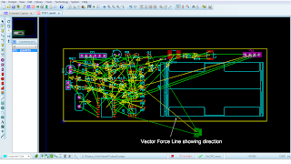
Now we want to add the JUMPER part on the board. As we move the component around the board before placing it the Vector Force line which is yellow colored shows direction where it could be placed. See the figure below-

Proteus Vector Force Tool
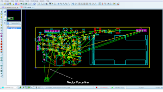
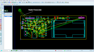
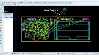
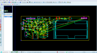
To understand more, move the component around and the vector force line will show you direction as shown in pictures below-

Proteus Vector Force Tool

This means that as you rotate the component around the board it provides visual guide for direction and placement. Note that the part can be moved around inside the board and this will give much more information for better placement.

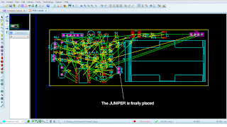
The figure below shows where the component was finally placed-

PCB component placement strategy
 

Selasa, 11 September 2012

Rotating parts in Proteus 8

Proteus 8 has a nice feature that it allows the shortcut keys to be customized according to your need. Proteus 8 uses + and - shortcut key for rotating parts/ components. But often you want another key such as "R" to use. So if you don't like some keyboard shortcut key you can change to any key in Proteus 8. This is a short tutorial that shows how to set the shortcut keys for rotating and can be applied to any other.

The steps are simple. Go to System menu and then select Set Keyword Mapping as shown-


This will bring up a a Edit Keyboard Map window that allows all the various shortcut key to be changed according to your preferences. Under the Command Groups, select Schematic Window Miscellaneous Command. Then under Available Commands select Rotate Clockwise and type in "R" in the Key sequence for selected command. Click Assign and finish up by clicking OK button. This is as shown-


Thats it. Now we can rotate the part by just clicking "R".

Senin, 10 September 2012

Comments on some Circuit Board Design Software

Circuit board design software also known as PCB design software is an essence in today's electronic design automation. With rapidly growing electronic industry and competitive market all electronic manufacturing companies relies on best circuit board design software.

What are the common circuit board design software? Which one is the best? Which should I use? Which is easy to learn? are some of the question many new comers ask today. These are important question.

Some of these question will be partially answered here and providing some guidance to new comers. There are over 50 EDA, free and proprietary that does PCB design and a complete list can be found in Wikipedia. Having said that below are names of commonly used and widely known circuit board software on which will be commented.
  • Cadence
  • Mentor Graphics
  • Altium designer
  • Proteus Professional
  • Eagle
What follows are some comments on these software and detailed differences and advantages would make a whole book.

Cadence Orcad/Allegro is perhaps the most popular, widely accepted PCB design software. It has wide range of feature. Cadence is integrated tool comprised of Orcad capture, Pspice and Allegro. Orcad capture is the schematic design tool, Pspice is the underlying simulation simulator and Allegro is the PCB design tool.

It is much matured and older circuit board design software. This means that tutorials, circuit designs, component footprints, schematic pars etc availability is much more making this software easier to learn in this regard. Extra features and tools like FPGA codesign, export/import and translator to other EDA, signal explorer, planner and architect, model integrity tools for creating IBIS model and other tools are available with this software. Thus it is a complete circuit board design software.

The drawback of this software maybe that it is comparatively little bit harder to learn than altium designer or proteus professional. 3D view of component with rotation and zoom view is not supported as in Altium Designer but provides 2D view. Another difference would be that of schematic editor window, the pcb design window, library editor opens in a separate window unlike in Altium designer in which schematic, pcb editor, library editor opens in same but new tabs making it a little bit easy(a relative view) to navigate between them. The zoom in/out feature of altium designer is better with mouse scrolling to different parts in schematic and pcb layout.

Altium designer like cadence also supports all tools required for designing a circuit board. Perhaps it is easier to understand then Cadence. The 3D model view of parts makes it easy for designer to create an image of what and how the final design will look like. The integrated library feature that ties up component schematic part, library part, simulation part, signal integrity and simulation part makes it easy for users to refer the component and removes the requirement to locate and browse the different parts files. Creating schematic part, footprint may also be easier than with cadence. Again the underlying simulator is a variant of spice. The work process of transfer from schematic to PCB is easier than Cadence. The placement of parts during the PCB board design is also easier. However perhaps the auto routing feature is not as useful as in Cadence.

Proteus Professional is much lighter PCB design software. The ISIS is for schematic design, the ARES for PCB design and VMS for microprocessor and FPGA based projects. The power and distinguishing feature of Proteus comes from interactive simulation, debugging with micro-controllers and microprocessors. This is very useful in projects with microprocessor and microcontroller based projects. Another feature of proteus is the visual indicator that guides designer in schematic wiring and pcb layout.

Sabtu, 08 September 2012

How to create Integrated Library in Altium Designer

This is a overall tutorial on how to create an integrated library in Altium designer. Integrated library is one unique feature of Altium designer that allows users to have an integrated library of schematic symbol, footprint, simulation model, signal integrity file and 3D view of the component. This way designers can quickly have a unified library of a component instead of having distributed parts in different folder.

There are number of ways to create Integrated Library file(<filename>.IntLib). One of them is to create a new package library(.PkgLib), add the schematic library(.SchLib)with schematic model, footprint library(.PcbLib) with footprint and other files(simulation, signal integrity, 3D) and compile the package library into integrated library file. Thus package lib file is one that binds the various model files into a single integrated library file.

Thus the first step is to create an Integrated library project. To do this follow the steps below-

1. Create a new Integrated Library
New > Project > Integrated Library as shown-


As shown below library package file with default name "Integrated_Library1.LibPkg" will be created in the project navigation bar.


It is good practice to save the project with some identifying name first. Right click on the "Integrated_Library1.LibPkg" and select "Save Project As" as shown-


Now provide some name such as "part_name_library" and browse to some location in your drive and click on "save" to save it there.


Now the integrated library project will be saved with the new "part_name_library" name and this change will also be reflected in the project navigation window as shown-


2. Add new schematic library to the integrated library project.

The next step is to add new schematic library to the integrated library project. To do this, right click on the part_name_library.LibPkg and select "Add New to Project" and from there select "Schematic_Library" as shown-


This will add a new schematic library document which will be visible under the part_name_library.LibPkg in the project navigation bar and the schematic editor window is visible-


Now to rename it and save it, right click on the schlib1.SchLib and click on "Save As" and enter some name like "part_sch_library" as shown below-


Now the name has changed as shown below-


Now click on the SCH library tab at the bottom right as shown-


This will bring up the SCH library panel shown below


It is here where we can draw the graphical symbol for the schematic component.

Here we have option to draw a new schematic component or copy and paste existing one. This is a tutorial on how to create an integrated package library rather than creating a new component from the scratch.

For illustration purpose the schematic symbol of 2N3904 is used here. After drawing the schematic NPN symbol for 2N3904 looks like the figure below-


Click on Tool > Rename Component and type in 2N3904. This will change the component name as reflected in the schematic library-


 Now the footprint, simulation model, signal integrity and PCB3D file can be added. The footprint and simulation model will be added here. Same process is used to add the signal integrity model file and the PCB3D file.

To add the footprint, click on the "Add Footprint" in the buttom panel as shown-


The PCB Model window will open that allows to select the footprint to attach from the listed footprint or by browsing to the directory where the desired footprint is located. For this tutorial, the footprint TO-92A that is required is located in the same folder as project folder. Browsing and selecting the footprint is shown below-


and then by setting the path for the project folder, the files in the path will be shown-


Select the footprint "2N3904.PcbLib" as shown-


After selecting the footprint the name and description will change-


Click ok and the footprint is now attached to the schematic library part as shown-


Similarly to add the simulation model file, click on the small select buttom near the Add Footprint as shown in figure below and select "Simulation"-

Then select Simulation-


This brings up the window to select the simulation model file. Click on browse and select the simulation model 2N3904.mdl as shown-

This bring up the another window where we can check the selected simulation model and confirm. Click OK.


Now the simulation model is also added as shown-


In this way the signal integrity file and the PCB3D file can be added.

Now to compile the package library go to the project. Select and right click the "part_name_library.LibPkg" and click on "Compile Integrated Library part_name_library.LibPkg" as shown-

The next window ask to save, click on OK to complete the creation of integrated library for the transistor.

After this a folder called ProjectOutputs is created automatically and the newly created Integrated Library File is resides within it as shown-


Now to use the newly created Integrated Library open a schematic sheet and select Part. Browse and add the newly created integrated library. This is as shown-


Place the Component onto the schematic sheet and the component is ready to be used.


This completes the tutorial.


Minggu, 02 September 2012

PCB design Tips

PCB design is a complicated work that is mastered by years of on-hand experience. This is due to the fact that electronic design inherently requires knowledge of many design areas. For example there are many choices of PCB laminates, conductors, number of planes etc that can be chosen according to the need of the product. Furthermore the design involves different types of electronics circuit- analog RF front end, digital, mixed type involving FPGA, microprocessors etc. Mechanical factors and environmental factors are other important design consideration. PCB designer face with these challenges with aim to produce cost effective and electrical, mechanical and environmental stable design.

Complete PCB design consideration can take complete book by itself, so it is not the intent here to discuss all the PCB design aspects but to provide concise part of important issues to be taken into account especially by beginners.

General Consideration and planning before starting PCB design:
  1. Board size, the environment
  2. Border lines 
  3. Mechanical mounting within 25mm from edges
  4. Connectors
  5. Conductor dimension(Resistance, Capacitive coupling, Inductor coupling)
General consideration for component placement
  1. Place mechanical mounting support, connectors, LED, heat sink
  2. Divide the circuit into functional units and subunits
  3. Place critical and larger components by adhering to the signal flow as much as possible
  4. Place smaller components in between the larger components
  5. Isolate inductive components, magnetic field generators, transformers from other components
  6. Place high frequency component together
  7. Avoid placing switch mode power supply near the ADC, DAC and analog circuitry
  8. Use separate voltage regulator for analog circuitry
  9. Be aware that PLDs and VLSI chips can generate switching current that infliterate into other components. Place bypass capacitors at their pins.
  10. Orient Polarized Parts such as diodes and electrolytic caps in the same direction
General consideration for conductors
  1. Determine the conductor dimension and spacing between them and other components
  2. Conductor width and spacing cannot be smaller than 4mils(0.1mm)
  3. Do not make conductors allow to make sharp angle bends
  4. Draw tracks along Y-axis in component side and tracks along X-axis on solder side in a double sided PCB
  5. Make the ground and power conductors width larger(Ground>Power>Signal)
  6. Make ground conductor capacity such that it can withstand different power supply load
  7. For high speed mixed circuitry use separate power and ground planes
  8. Spacing between power and ground conductors should be large as possible to avoid cross-talk
  9. Ground plane is necessary in all high frequency design

    Sabtu, 01 September 2012

    Difference between Non-Plated and Plated Through Holes

    During PCB design many issues come across and one of them is in the regard of non-plated and plated through holes. What is the difference between them and where should one use which one? is a commonly asked question. Here we will briefly discuss this issue.

    Through hole components have leads(straight or clinched) and these leads are put through holes available or made on the PCB insulating materials and soldered on the other side onto the copper tracks.

    The difference between non plated through hole and plated through hole is the presence of plated copper inside the insulating base material as shown in the pictures below. The presence of this plated through hole has in turn effect on electrical properties and mechanical stability. When component leads is soldered through plated holes then (1)the electrical resistance by the joint formed becomes less and (2) the mechanical stability increases. This is not the case with the non plated holes and hence plated through holes are more beneficial than non plated through hole joints.

    Other differences include the cost and area. Plated through holes PCB is more costly than the non-plated through hole PCB. And plated through holes PCB consumes less space/area than the non-plated through hole PCB.

    The advantage of using non plated through holes come from simpler and maybe quicker manufacturing.

    The figure below shows the non plated through hole and plated through hole where straight leads of component is used.
    Non-plated through hole with straight lead
    Fig 1: Non-plated through hole with straight lead

    Plated through hole with straight lead
    Fig 2: Plated through hole with straight lead

    Printed Circuit Board Categories

    A printed circuit board(PCB) is a board used to hold electronic part assembly by soldering them onto the board. PCBs are made up of various forms of insulating materials such as woven glass fabric reinforced by epoxide resin or polyimide forms and others. The electronics parts IC, resistors, capacitors are connected with copper tracks that are printed onto the PCB. The PCB can be produced with different architecture depending primarily upon the necessity of density of electronic component to be soldered to reduce cost.

    Broadly we can classify PCB architecture into 3 categories or types as follows:
    1. Single Sided PCB
    2. Double Sided PCB
    3. Multilayer PCB
    1. Single Sided PCB

    The picture below shows single sided PCB

    Single Sided PCB
    Fig 1: Single Sided PCB
     In Single PCB, components are placed on one side of the board and the copper tracks are printed on the another side. The components are connected to the copper tracks via holes through the board.
     
     2. Double Sided PCB

    The picture below shows double sided PCB

    Double Sided PCB
    Fig 2: Double Sided PCB
     In Double Sided PCB, components and copper tracks are found on both sides of the board. However usually, components are placed on one side and tracks on top and bottom are interconnected with plated through vias. With surface mounted components, they may also be placed on either side of the board and tracks are also printed on both sides of the board with interconnection between them using plated through vias.

    3. Multilayer PCB

    The picture below shows multilayer PCB

    Multilayer PCB
    Fig 3: Multilayer PCB
    Multilayer PCB is one made up of more than 3 layers of insulating board. When top and bottom copper tracks are to be interconnected plated through vias are used. And when copper tracks inside the middle boards are to be connected either to the other middle layer board or top or bottom layer copper tracks then burried vias or blind vias are used.