In this Altium Designer tutorial an AM circuit schematic will be designed and simulated. The final AM circuit that will be designed is shown below.
Circuit Explanation:
In this simple AM circuit shown, there are two transistors Q1 and Q2 (2N3904). The transistor Q1 is part of oscillator that generates carrier signal while Q2 performs modulation of the input signal shown as sine_signal with the carrier signal from the Q1. The output at the collector of Q2 is the AM signal(in figure labelled AMsignal).
The resistors R2, R4 and R5 are to bias the transistor Q1 and the inductor L1 together with capacitors C7 and C10 forms the tank of the oscillator. C1 is the bypass capacitor. The RF signal at the collector of Q1 drives the modulator or buffer stage Q2. The inductor L2 together with capacitors C6 and C8 forms the tank circuit for the buffer. The AM RF signal appears at the junction of C6 and C8. The resistor R6 is just the arbitrary load resistor.
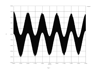
The output AM waveform is as shown below-
The AM schematic with the battery, input port and the load resistor removed is below-
Now to create the PCB layout for this design, PCB wizard that is available in Alitum Designer will be used. For this goto, System > Files, and then click on PCB Board Wizard from the New from Template.
It then displays an introduction page, clicking next brings up the dimension unit to be used. Here select "metric" because we will be working with mm. This then brings up a list of various standard board layout that can be chosen or you can enter your custom board size.
 |
| Fig: AM circuit design with Altium Designer |
In this simple AM circuit shown, there are two transistors Q1 and Q2 (2N3904). The transistor Q1 is part of oscillator that generates carrier signal while Q2 performs modulation of the input signal shown as sine_signal with the carrier signal from the Q1. The output at the collector of Q2 is the AM signal(in figure labelled AMsignal).
The resistors R2, R4 and R5 are to bias the transistor Q1 and the inductor L1 together with capacitors C7 and C10 forms the tank of the oscillator. C1 is the bypass capacitor. The RF signal at the collector of Q1 drives the modulator or buffer stage Q2. The inductor L2 together with capacitors C6 and C8 forms the tank circuit for the buffer. The AM RF signal appears at the junction of C6 and C8. The resistor R6 is just the arbitrary load resistor.
The output AM waveform is as shown below-
 |
| AM waveform |
Now to create the PCB layout for this design, PCB wizard that is available in Alitum Designer will be used. For this goto, System > Files, and then click on PCB Board Wizard from the New from Template.
It then displays an introduction page, clicking next brings up the dimension unit to be used. Here select "metric" because we will be working with mm. This then brings up a list of various standard board layout that can be chosen or you can enter your custom board size.


Tidak ada komentar:
Posting Komentar