This video tutorial shows simulation of ASK modulation using Orcad Capture. Message is in the form of unipolar binary stream and is impressed on a high frequency carrier wave with frequency 100KHz. The output is a ASK signal which is shown in graph.
Rabu, 31 Oktober 2012
ASK modulation using Orcad Capture
ASK modulation is digital modulation technique wherein binary message signal stream is impressed onto the high frequency carrier signal for transmission over larger bandwidth channels such as air. The binary message signal stream is of unipolar type, that means that 1V represents logical 1 and 0V represents the logical 0 bit. The binary message stream turns On/Off the modulator such that the high frequency carrier signal is transmitted when modulator is switched on and during the off state nothing is transmitted.
In orcad capture a voltage controlled switch called Sbreak can be used to stimulate the behavior of the modulator. In reality a modulator is made of transistors that switches on/off in response to clock impulses supplied to it.
The schematic for simulating ASK modulation is shown in figure below-
In the schematic, the message signal labelled Message_Signal is a binary unipolar signal with V1=0V and V2=1V, TD=0s, TR=0.01us, TF=0.01us, PW=30us and PER=90us. The carrier signal labelled Carrier_Signal is a sinusoid with amplitude VAMPL=10V and frequency of 100KHz. The message binary sequence turns on/off the switch and carrier signal is transmitted as ASK signal labelled ASK_Signal. The 1k load resistance at the output simulates the resistance of the switch(modulator).
The simulation setting is shown in the figure below-
The output graph shown below shows the result of the simulation. The top graph is the binary message signal, the middle graph is the carrier signal waveform and the bottom graph is the ASK signal waveform.
Also see ASK Modulation Video Tutorial
Download ASK modulation simulation files:
http://www.filefactory.com/file/33tovaqoj98f/ASK_zip
For Phase modulation tutorial- see PSK modulation using orcad capture
In orcad capture a voltage controlled switch called Sbreak can be used to stimulate the behavior of the modulator. In reality a modulator is made of transistors that switches on/off in response to clock impulses supplied to it.
The schematic for simulating ASK modulation is shown in figure below-
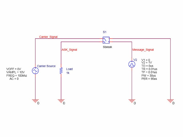 |
| Fig: ASK modulation schematic |
The simulation setting is shown in the figure below-
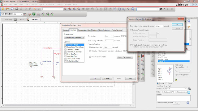 |
| Fig: Simulation setting for ASK modulation |
The output graph shown below shows the result of the simulation. The top graph is the binary message signal, the middle graph is the carrier signal waveform and the bottom graph is the ASK signal waveform.
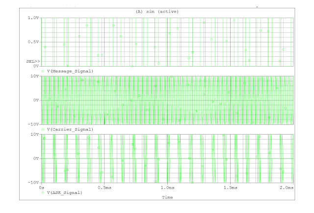 |
| Fig: ASK modulation simulation output graph |
Download ASK modulation simulation files:
http://www.filefactory.com/file/33tovaqoj98f/ASK_zip
For Phase modulation tutorial- see PSK modulation using orcad capture
Bit Rate and Bit Duration Calculation for PCM modulation
The PCM(Pulse Code Modulation) refers to the process of converting analog signal. The analog signal such as speech is usually the input signal. The whole process of converting the analog signal to digital form involves 4 steps-
Filtering
Filtering involves passing the analog signal through a filter called the anti-aliasing filter that allows selected portion of signal energy/ power to pass and stops other signal energy/ power to pass through the filter. This is done to avoid overlapping of samples and produce ISI(Inter-Symbol Interference) Effect.
- Filtering
- Sampling
- Quantization
- Encoding
Filtering
Filtering involves passing the analog signal through a filter called the anti-aliasing filter that allows selected portion of signal energy/ power to pass and stops other signal energy/ power to pass through the filter. This is done to avoid overlapping of samples and produce ISI(Inter-Symbol Interference) Effect.
Sampling
The sampling is performed on the output of the filter using sample and hold circuit. The sample and hold circuit consists of transistors that are turned on/off using periodic clocked pulse. On one input port the signal from the filter is fed into the sample and hold circuit and another another clocked pulse input is fed from another input port. The frequency of the clock is the sampling frequency that turns ON/Off the transistors. As a result of this sampled PAM signal is produced at the output of the sample/hold circuit.
Quantization
The sampled PAM signal is quantized into discrete level. Each discrete level has a corresponding binary bit values. At each sampling instant, portion of the analog PAM signal is quantized to the nearest level and corresponding binary bit values appears at the output. In PCM, 8 bits/sample are used and sampled at the rate of 8Khz sample/sec (i.e sampling rate=Fs=8Khz).
The number of levels is \[L=2^{n}=2^{8}=256\] levels.
The PCM bit rate is-
\[R_{b}={sample/sec}\times{bits/sample}\]
That is,
\[R_{b}={8Khz}\times{8bits/sample}=64kbps\]
The sampling time is-
\[T_s=1/F_s=1/8Khz=125\mu{s}\]
This means that every 125 micro-second, 8bits representing the analog signal sample comes out of the quantizer.
The bit duration of each of the 8 bit is then-
\[T_b=T_s/8=125\mu{s}/8=15.625\mu{s}\]
Encoding
Encoding process is the selection of and implementation of various available encoding format. Example includes Polar, Bipolar which may be RZ or NRZ types(see analysis of Analysis of Polar, Bipolar, NRZ and RZ baseband encoding), AMI Bipolar encoding, Manchester encoding etc. The selection of encoding format depends upon the application and requirement such as error detecting capability, synchronization capability, cost of circuit implementation etc.
Senin, 29 Oktober 2012
Implementation of Huffman Coding
This is a second part and continuation of Huffman encoding/decoding implementation in Xilinx ISE project. For the first part see Huffman Encoder/Decoder using Xilinx ISE. If readers require Xilinx ISE, visit this blogpost download Xilinx ISE v14.6 or download Xilinx ISE v14.3.
3. Implementation of Huffman Coding
3.1 Huffman Implementation on Xilinx FPGA for MPEG 2:
The following block diagram shows the implementation of Huffman coding on Xilinx:
3.2 Tables for Encoder & Decoder:
The following tables are the variable length code tables or LUT for Huffman implementation:
1. Table for Quantization Level:
2. VCL Table for Encoding DC coefficients a. Luminance VCL Table
b. Chrominance VCL Table
3. VCL Table for Encoding AC coefficients a. Non Intra-Coded Blocks
b. Intra Coded Blocks
4. Table for Decoding DC coefficients
5. Table for Decoding AC coefficients
1. Table for Quantization Level:
2. VCL Table for Encoding DC coefficients
a. Luminance VCL Table
b. Chrominance VCL Table
3. VCL Table for Encoding AC coefficients:
a. Non Intra-Coded Blocks
b. Intra-Coded Blocks
4. Table for Decoding DC coefficients:
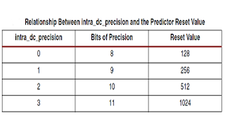
Three predictor values are maintained for each color component. The predictor values are set at the start of the slice, or when a non-intra macroblock is decoded, or when a macroblock is skipped. The predictor values for different intra_dc_precisions are shown in Table below:
5. Table for Decoding AC coefficients:
The run/level pair is decoded from the Huffman code using a look-up table (LUT). There are three possible options for the Huffman code. If the code represents an EOB, all the remaining coefficients are set to "0". If the code represents an escape code, the next six bits represent the run and the following 12 bits represent the level. If the VLC denotes a normal coefficient, then the run coefficients are set to zero and the following level coefficient is set to the level value depending on the value of s. When s == 0, the signed level is the same as level. When s == 1, the signed level is equal to (–level).
Huffman Encoder/Decoder using Xilinx ISE
This article explains in details the steps involved in FPGA implementation of Huffman Encoder/ Decoder using Xilinx ISE software. First the background theory part that is essential is explained and then the actual FPGA implementation of the encoder/ decoder is provided. Also provided herewith is the VHDL code for the Huffman encoder/ decoder. If readers require Xilinx ISE, visit this blogpost download Xilinx ISE v14.6 or download Xilinx ISE v14.3.
1. Huffman Coding Algorithm
Huffman coding is used to code values statistically according to their probability of occurrence. Short code words are assigned to highly probable values and long code words to less probable values. Huffman coding is used in MPEG-2 to further compress the bit stream. This system describes how Huffman coding is done in MPEG-2 and its implementation.
1.1 Algorithm
1. Reduce the source S to S1 and continue on to S2, S3 until we reach a source with two
symbols (or one for which it is easy to design a compact code).
2. Assign a compact code for the final reduced source. For a two symbol source the trivial code is a 0 and 1.
3. Backtrack to the original source assigning a compact code for the jth reduced source . The compact code we assign to the original source is the binary Huffman code.
1.2 Steps
1. Adding the two least probable symbols gives 25%. The new symbol is F
2. Adding the two least probable symbols gives 45%. The new symbol is G
3. Adding the two least probable symbols gives 55%. The new symbol is H
4. Write "0" and "1" on each branch of the summation arrows. These binary values are called branch binaries.
5. For each letter in each column, copy the binary numbers from the column on the right, starting from the right most columns (i.e., in column three, G gets the value "1" from the G in column four.) For summation branches, append the binary from the right-hand side column to the left of each branch binary. For A and C in column three append "0" from H in column four to the left of the branch binaries. This makes A "00" and B "01".
Completing step 5 gives the binary values for each letter: A is "00", B is "01", C is "11", D is "100", and E is "101". The input with the highest probability is represented by a code word of length two, whereas the lowest probability is represented by a code word of length three.
2. Block Diagram & Architecture of Huffman Coding
2.1 Encoding
The following block diagram shows the key processing steps of encoding.
Processing Steps
1. Application of DCT to the video/image stream
Source image samples are grouped into 8x8 blocks, shifted from unsigned integers to signed integers and input to the DCT. The following equation is the idealized mathematical definition of the 8x8 DCT:
1. Application of DCT to the video/image stream
Source image samples are grouped into 8x8 blocks, shifted from unsigned integers to signed integers and input to the DCT. The following equation is the idealized mathematical definition of the 8x8 DCT:
Each 8x8 block of source image samples is effectively a 64-point discrete signal which is a function of the two spatial dimensions x and y. The DCT takes such a signal as its input and decomposes of the 64 unique two-dimensional "spatial frequencies" which comprise the input signal's "spectrum." The output of the DCT is the set of 64 basis-signal amplitudes (DCT coefficients) whose values can be regarded as the relative amount of the 2D spatial frequencies contained in the 64-point input signal.The DCT coefficients are divided into "DC coefficient" and "AC coefficients". DC coefficient is the coefficient with zero frequency in both dimensions, and AC coefficients are remaining 63 coefficients with non-zero frequencies. The DCT step can concentrate most of the signal in the lower spatial frequencies. In others words, most of the spatial frequencies have zero or near-zero amplitude and need not be encoded. Because the DCT equations contain transcendental functions, no physical implementation can compute them with perfect accuracy. Besides, JPEG does not specify unique DCT algorithm in its proposed standard. This, however, makes compliance more difficult to confirm since two compliant encoders (or decoders) generally will not produce identical outputs given identical inputs.
2. Quantization
To achieve further compression, each of the 64 DCT coefficients is uniformly quantized
in conjunction with a 64-element Quantization Table, which is specified by the application. The purpose of quantization is to discard information which is not visually significant.. Because quantization is a many-to-one mapping, it is fundamentally lossy. Moreover, it is the principal source of lossyness in DCT-based encoder.Quantization is defined as division of each DCT coefficient by its corresponding quantizer step size, followed by rounding to the nearest integer, as following equation:

and then the output is normalized by the quantizer step size.
Each step size of quantization ideally should be chosen as the perceptual threshold to compress the image as much as possible without visible artifacts. It is also a function of the source image characteristics, display characteristics and viewing distance.
2. Quantization
To achieve further compression, each of the 64 DCT coefficients is uniformly quantized
in conjunction with a 64-element Quantization Table, which is specified by the application. The purpose of quantization is to discard information which is not visually significant.. Because quantization is a many-to-one mapping, it is fundamentally lossy. Moreover, it is the principal source of lossyness in DCT-based encoder.Quantization is defined as division of each DCT coefficient by its corresponding quantizer step size, followed by rounding to the nearest integer, as following equation:

and then the output is normalized by the quantizer step size.
Each step size of quantization ideally should be chosen as the perceptual threshold to compress the image as much as possible without visible artifacts. It is also a function of the source image characteristics, display characteristics and viewing distance.
3. Entropy Encoding
The final processing step of encoder is entropy coding. Before entropy coding, there are a
few processing steps for the quantized coefficients. Note that the DC coefficient is treated separately from the 63 AC coefficients. The DC coefficients are a measure of the average value of the 64 image samples. Because there is usually strong correlation between the DC coefficients of adjacent 8x8 blocks, the quantized DC coefficient is encoded as the difference from the DC term of the previous block in the encoding order, called Differential Pulse Code Modulation ( DPCM ), and the function is as followed :
few processing steps for the quantized coefficients. Note that the DC coefficient is treated separately from the 63 AC coefficients. The DC coefficients are a measure of the average value of the 64 image samples. Because there is usually strong correlation between the DC coefficients of adjacent 8x8 blocks, the quantized DC coefficient is encoded as the difference from the DC term of the previous block in the encoding order, called Differential Pulse Code Modulation ( DPCM ), and the function is as followed :
DiffDC(i) = DC(i) - DC(i-1)
where i is the i-th block, DC(0) = 0
DPCM can usually achieve further compression due to the smaller range of the coefficient values. The remaining AC coefficients are ordered into the "zig-zag" sequence, which helps to facilitate entropy coding by placing low-frequency coefficients before high-frequency coefficients.
Now the outputs of DPCM and "zig-zag" scanning can be encoded by entropy coding separately. It encodes the quantized DCT coefficients more compactly based on their statistical characteristics.
Entropy coding can be considered as 2-step process. The first step converts the zig-zag sequence of quantized coefficients into an intermediate sequence of symbols. The second step converts the symbols to a data stream in which the symbols no longer have externally identifiable boundaries. The form and definition of the intermediate symbols is dependent on both the DCT-based mode of operation and the entropy coding method.
Entropy coding can be considered as 2-step process. The first step converts the zig-zag sequence of quantized coefficients into an intermediate sequence of symbols. The second step converts the symbols to a data stream in which the symbols no longer have externally identifiable boundaries. The form and definition of the intermediate symbols is dependent on both the DCT-based mode of operation and the entropy coding method.
2.2 Decoding
The block Diagram shows decoding processing steps:
1. Entropy Decoding
Similar to entropy coding, entropy decoding also can be considered as 2-step process.
The first step converts the input bit stream into the intermediate symbols. The second step converts the intermediate symbols into the quantized DCT coefficients. In fact, the output of the second step is the DC difference, the output of DPCM, and the AC coefficients after zig-zag scan. Therefore, the DC difference is then decoded into the quantized DC coefficient, and the AC coefficients are ordered into original order.
2. De-Quantization
The following step is to de-quantize the output of entropy decoding, returning the result
to a representation appropriate for input to the IDCT. The equation is as follow-
3. Inverse Discrete Cosine Transform (IDCT)
The last step of decoder is the IDCT. It takes the 64 quantized DCT coefficients and
reconstructs a 64-point output image signal by summing the basis signals. JPEG does not specify a unique IDCT algorithm in its standard either. The mathematical definition of the 8x8 IDCT is as follow-
Sabtu, 27 Oktober 2012
PTC MathCAD Prime 2 download free
PTC MathCAD Prime is an engineering software that can be used to analyze, solve and share engineering calculation, critical design ideas. Download PTC MathCAD Prime for free here from the download link below.
Complex Mathematical equations can be solved easily and plotted on 23, 3D graphs to get a geometric visualization from which idea can be obtained. Mathematical problems such as partial differential equations and ordinary partial differential equations, root polynomials, system of equations, vector and matrix, curve fitting and regression analysis can be solved using this engineering software.
Complex Mathematical equations can be solved easily and plotted on 23, 3D graphs to get a geometric visualization from which idea can be obtained. Mathematical problems such as partial differential equations and ordinary partial differential equations, root polynomials, system of equations, vector and matrix, curve fitting and regression analysis can be solved using this engineering software.
Download Link for MathCad Prime 2.0:
http://rapidgator.net/file/79125210/PMP2.0M010.part1.rar.html
http://rapidgator.net/file/79125211/PMP2.0M010.part2.rar.html Kamis, 25 Oktober 2012
Xilinx ISE Download free
Download Xilinx ISE v14.6 the latest version of Xilinx software for free here. Xilinx ISE Design Suite is a software for designing Programmable Logic Devices or FPGA. It allows FPGA devices prototyping using HDL languages such as verilog and VHDL, simulation and timing verification. Once the device has been designed it can be used to create a physical FPGA device. Example of application of Xilinx ISE software in the field of communication system development is the design and verification of source encoder/ decoder such as Huffman encoding algorithm, channel encoder, MPEG and video compression algorithms.
Also see the FPGA design tutorials here in this blog.
Also see the FPGA design tutorials here in this blog.
Selasa, 23 Oktober 2012
Download Virtual Serial Port Emulator for Free
Download Eltima Virtual Serial Port Emulator here. This software allows electronics and communication system designer to create and simulate a serial comport communication. This is required during the prototyping of electronics system for example when a microprocessor/microcontroller and to be interfaced with the PC serial com port. This free virtual serial port emulator is helpful in such design cases. It allows designers to create the virtual comport without actually physically wiring of the comport and check and visualize the working of the serial communication. Design scenario includes creating a virtual serial port for ethernet to serial or serial to ethernet, USB to RS485 or RS232 serial interface. This popular Eltima Virtual Serial Port Emulator is for free download
Download links for Virtual Serial Port Emulator:
or,
Download links for Virtual Serial Port Emulator:
http://extabit.com/file/2cqzkhaa3crxx or,
http://netload.in/datei3v0Ocw3Ieb/Eltima.Software.Virtual.Serial.Port.Driver.v7.1.KeyGen-TPoDT.rar.htmJumat, 19 Oktober 2012
Electrotechnical System with Mathematica and Pspice Free Download
Ringkasan ini tidak tersedia. Harap
klik di sini untuk melihat postingan.
Kamis, 18 Oktober 2012
Download Modern VLSI Design by Wayne Wolf Ebook Free
 Download Ebook Free- Modern VLSI Design: IP based Design fourth edition by Wayne Wolf. This book on VLSI design is one of the popular book in VLSI technology used as text books in many graduate courses. This fourth edition is a refinements of earlier version and new topics are added. It is specially useful because it emphaisis on IP(Intellectual Property) based VSLI design approach. It contains digital design with VLSI overview, an introduction part. The chapters following this introduction are fabrication process of VLSI devices, logic gates, computational logic networks, sequential machines, subsystem design, floor-planning and architectural design.
Modern VLSI Design Free Download Link:
http://www.filefactory.com/file/42dplv2ztibz/n/mvlsi.pdfCommunication System Development using PIC16F84A Microcontroller using Proteus 8 and MpLAB
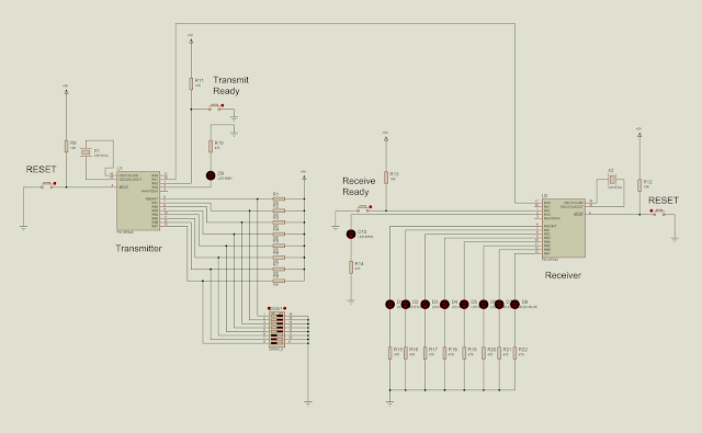
In this communication system project using Proteus 8 software a simple communication system is shown using two PIC16F84A microcontrollers which acts as a transmitter and receiver. Assembly code for the two microcontroller is provided and shown how these microcontroller communicate.
The basic communication is via a simple protocol which allows the two micro-controllers to communicate. The switches at the transmitter MC are used as input and converted to message and sent to the receiving microcontroller serially. The received message is then shown to light up the output leds at the receiver. In other words the state of the switches forms the message to be sent and the LED glow at the receiver forms the message received.
The Schematic for this communication system is shown below-
The components used are-
To generate the hex code open the MpLAB and create a new project by clicking on the Project>Project Wizard.
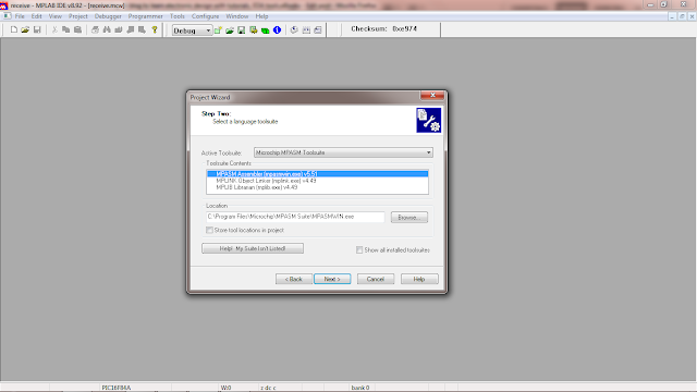
A new window will pop-up, click next. Then in the next window select PIC16F84A, then click next. In the language toolsuite option, select Microchip MPASM Toolsuite as shown-
In the next window step 3, select a folder where you want to save the project and the name of the project.
Then the step 4 allows you to add files to the project. Add the following files-
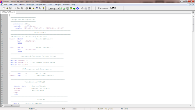
For the transmitter microcontroller, open the 16F84ATEMO.asm template just created by double clicking on it and copy-paste the below assembly code for the transmitter.
Transmitter Microcontroller Source Code:
;=========================
; setup and configuration
;=========================
processor 16f84A
include <p16f84A.inc>
__config _XT_OSC & _WDT_OFF & _PWRTE_ON & _CP_OFF
;============================================================
; M A C R O S
;============================================================
; Macros to select the register banks
Bank0 MACRO ; Select RAM bank 0
bcf STATUS,RP0
ENDM
Bank1 MACRO ; Select RAM bank 1
bsf STATUS,RP0
ENDM
;=====================================================
; constant definitions for pin wiring
;=====================================================
#define readySW 2 ;|
#define readyLED 3 ;| -- from wiring diagram
#define serialLN 0 ;|
;=====================================================
; PIC register and flag equates
;=====================================================
c equ 0 ; Carry flag
tmrOVF equ 2 ; Timer overflow bit
;
;======================================================
; variables in PIC RAM
;=====================================================
cblock 0x0c ; Start of block
bitCount ; Counter for 8 bits
rcvReg ; Data to send
temp
endc
;=========================================================
; program
;=========================================================
org 0 ; start at address
goto main
; Space for interrupt handlers
org 0x04
main:
Bank1
; Port A bits 0 and 2 are input. All others are output
movlw b'00000101' ; port A setup
movwf TRISA
; Port B is all output
movlw b'00000000' ; port B setup
MOVWF TRISB
Bank0
; Turn off all port B LEDs
clrf PORTB
; And receiver register
clrf rcvReg
; Prepare to set prescaler
clrf TMR0
clrwdt
; Setup OPTION register for full timer speed
movlw b'11011000'
; 1 1 0 1 1 0 0 0 <= OPTION bits
; | | | | | |__|__|_____ PS2-PS0 (prescaler bits)
; | | | | | Values for Timer0
; | | | | | *000 = 1:2 001 = 1:4
; | | | | | 010 = 1:8 011 = 1:16
; | | | | | 100 = 1:32 101 = 1:64
; | | | | | 110 = 1:128 111 = 1:256
; | | | | |______________ PSA (prescaler assign)
; | | | | *1 = to WDT
; | | | | 0 = to Timer0
; | | | |_________________ TOSE (Timer0 edge select)
; | | | 0 = increment on low-to-high
; | | | *1 = increment in high-to-low
; | | |____________________ TOCS (TMR0 clock source)
; | | *0 = internal clock
; | | 1 = RA4/TOCKI bit source
; | |_______________________ INTEDG (Edge select)
; | 0 = falling edge
; | *1 = raising edge
; |__________________________ RBPU pullups
; 0 = enabled
; *1 = dissabled
option
; Dissable interrupts
bcf INTCON,5 ; Timer0 overflow dissabled
bcf INTCON,7 ; Global interupts dissabled
;=========================
; wait for READY switch
; to be pressed
;=========================
ready2rcv:
btfsc PORTA,readySW ; Test switch
goto ready2rcv ; loop
; Turn ON the ready-to-receive LED
bsf PORTA,readyLED
;===========================
; receiving
;===========================
call rcvData ; Call serial input procedure
;===========================
; data received
;===========================
; Turn ready to receive LED off
bcf PORTA,readyLED
; Display received data
movf rcvReg,w ; Byte received to w
movwf PORTB ; display in port B
;===========================
; wait forever
;===========================
endloop:
goto endloop
;============================================================
; procedure to receive serial data
;============================================================
; ON ENTRY:
; local variable dataReg is used to store 8-bit value
; received through port (labeled serialLN)
; OPERATION:
; 1. The timer at register TMR0 is set to run at
; maximum clock speed, that is, 256 clock beats.
; The timer overflow flag in the INTCON register
; is set when the timer cycles from 0xff to 0x00.
; 2. When the START signal is received, the code
; waits for 128 timer beats so as to read data in
; the middle of the send period.
; 3. Each bit (start, data, and stop bits) is read
; at intervals of 256 timer beats.
; 4. The procedure tests the timer ofverflow flag
; (tmrOVF) to determine when the timer cycle has
; ended, that is when 256 clock beats have passed.
;------------------------------------------------------------
rcvData:
clrf TMR0 ; Reset timer
movlw 0x08 ; Initialize bit counter
movwf bitCount
;=========================
; wait for START bit
;=========================
startWait:
btfsc PORTA,0 ; Is port A0 low?
goto startWait ; No. Wait for mark
;=========================
; offset 128 clock beats
;=========================
; At this point the receiver has found the falling
; edge of the start bit. It must now wait 128 timer
; beats to synchronize in the middle of the sender's
; data rate, as follows:
; |<========= falling edge of START bit
; |
; |-----|<====== 128 clock beats offset
; ----------. | .---------
; | | <== SIGNAL
; -----------
; |<-- 256 -->|
;
movlw 0x80 ; 128 clock beats offset
movwf TMR0 ; to TMR0 counter
bcf INTCON,tmrOVF ; Clear overflow flag
offsetWait:
btfss INTCON,tmrOVF ; timer overflow?
goto offsetWait ; wait until
btfsc PORTA,0 ; Test start bit for error
goto offsetWait ; Recycle if a false start
;==========================
; receive data
;==========================
clrf TMR0 ; Restart timer
bcf INTCON,tmrOVF ; Clear overflow flag
; Wait for 256 timer cycles for first/next data bit
bitWait:
btfss INTCON,tmrOVF ; Timer cycle end?
goto bitWait ; Keep waiting
; Timer has counter 256 beats
bcf INTCON,tmrOVF ; Reset overflow flag
movf PORTA,w ; Read port A into w
movwf temp ; Store value read
rrf temp,f ; Rotate bit 0 into carry flag
rlf rcvReg,f ; Rotate carry into rcvReg bit 0
decfsz bitCount,f ; 8 bits received
goto bitWait ; Next bit
; Wait for one time cycle at end of reception
markWait:
btfss INTCON,tmrOVF ; timer overflow flag
goto markWait ; keep waiting
;========================
; end of reception
;========================
return
;=========================================================
; end of program
;=========================================================
end
Once copied click on Build All option to start compiling the assembly code. Once this is complete, it should show Build Succeeded as shown below-
This create a transmit.hex (transmit is the project name here) in the MpLAB project folder. See below-
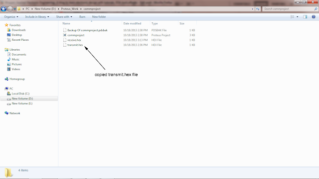
Copy the transmit.hex file into your microcontroller proteus project folder. See example below-
Now to burn the transmit.hex file to the transmitter microcontroller, go to the schematic and double click on the transmitter microcontroller to bring up its properties window. Then click on the folder icon and browse for the transmit.hex file and click ok to exit the window.
Now the transmitter microcontroller is ready for simulation.
Repeat the same steps for the receiver microcontroller by starting by creating a new MpLAB project, adding the same files, copying and pasting the receiver assembly code provided below, compiling and creating a receive.hex file and lastly uploading the hex file to the receiver microcontroller.
Receiver Microcontroller Source Code:
;=========================
; setup and configuration
;=========================
processor 16f84A
include <p16f84A.inc>
__config _XT_OSC & _WDT_OFF & _PWRTE_ON & _CP_OFF
;============================================================
; M A C R O S
;============================================================
; Macros to select the register banks
Bank0 MACRO ; Select RAM bank 0
bcf STATUS,RP0
ENDM
Bank1 MACRO ; Select RAM bank 1
bsf STATUS,RP0
ENDM
;=====================================================
; constant definitions for pin wiring
;=====================================================
#define readySW 2 ;|
#define readyLED 3 ;| -- from wiring diagram
#define serialLN 0 ;|
;=====================================================
; PIC register and flag equates
;=====================================================
c equ 0 ; Carry flag
tmrOVF equ 2 ; Timer overflow bit
;
;======================================================
; variables in PIC RAM
;=====================================================
cblock 0x0c ; Start of block
bitCount ; Counter for 8 bits
rcvReg ; Data to send
temp
endc
;=========================================================
; program
;=========================================================
org 0 ; start at address
goto main
; Space for interrupt handlers
org 0x04
main:
Bank1
; Port A bits 0 and 2 are input. All others are output
movlw b'00000101' ; port A setup
movwf TRISA
; Port B is all output
movlw b'00000000' ; port B setup
MOVWF TRISB
Bank0
; Turn off all port B LEDs
clrf PORTB
; And receiver register
clrf rcvReg
; Prepare to set prescaler
clrf TMR0
clrwdt
; Setup OPTION register for full timer speed
movlw b'11011000'
; 1 1 0 1 1 0 0 0 <= OPTION bits
; | | | | | |__|__|_____ PS2-PS0 (prescaler bits)
; | | | | | Values for Timer0
; | | | | | *000 = 1:2 001 = 1:4
; | | | | | 010 = 1:8 011 = 1:16
; | | | | | 100 = 1:32 101 = 1:64
; | | | | | 110 = 1:128 111 = 1:256
; | | | | |______________ PSA (prescaler assign)
; | | | | *1 = to WDT
; | | | | 0 = to Timer0
; | | | |_________________ TOSE (Timer0 edge select)
; | | | 0 = increment on low-to-high
; | | | *1 = increment in high-to-low
; | | |____________________ TOCS (TMR0 clock source)
; | | *0 = internal clock
; | | 1 = RA4/TOCKI bit source
; | |_______________________ INTEDG (Edge select)
; | 0 = falling edge
; | *1 = raising edge
; |__________________________ RBPU pullups
; 0 = enabled
; *1 = dissabled
option
; Dissable interrupts
bcf INTCON,5 ; Timer0 overflow dissabled
bcf INTCON,7 ; Global interupts dissabled
;=========================
; wait for READY switch
; to be pressed
;=========================
ready2rcv:
btfsc PORTA,readySW ; Test switch
goto ready2rcv ; loop
; Turn ON the ready-to-receive LED
bsf PORTA,readyLED
;===========================
; receiving
;===========================
call rcvData ; Call serial input procedure
;===========================
; data received
;===========================
; Turn ready to receive LED off
bcf PORTA,readyLED
; Display received data
movf rcvReg,w ; Byte received to w
movwf PORTB ; display in port B
;===========================
; wait forever
;===========================
endloop:
goto endloop
;============================================================
; procedure to receive serial data
;============================================================
; ON ENTRY:
; local variable dataReg is used to store 8-bit value
; received through port (labeled serialLN)
; OPERATION:
; 1. The timer at register TMR0 is set to run at
; maximum clock speed, that is, 256 clock beats.
; The timer overflow flag in the INTCON register
; is set when the timer cycles from 0xff to 0x00.
; 2. When the START signal is received, the code
; waits for 128 timer beats so as to read data in
; the middle of the send period.
; 3. Each bit (start, data, and stop bits) is read
; at intervals of 256 timer beats.
; 4. The procedure tests the timer ofverflow flag
; (tmrOVF) to determine when the timer cycle has
; ended, that is when 256 clock beats have passed.
;------------------------------------------------------------
rcvData:
clrf TMR0 ; Reset timer
movlw 0x08 ; Initialize bit counter
movwf bitCount
;=========================
; wait for START bit
;=========================
startWait:
btfsc PORTA,0 ; Is port A0 low?
goto startWait ; No. Wait for mark
;=========================
; offset 128 clock beats
;=========================
; At this point the receiver has found the falling
; edge of the start bit. It must now wait 128 timer
; beats to synchronize in the middle of the sender's
; data rate, as follows:
; |<========= falling edge of START bit
; |
; |-----|<====== 128 clock beats offset
; ----------. | .---------
; | | <== SIGNAL
; -----------
; |<-- 256 -->|
;
movlw 0x80 ; 128 clock beats offset
movwf TMR0 ; to TMR0 counter
bcf INTCON,tmrOVF ; Clear overflow flag
offsetWait:
btfss INTCON,tmrOVF ; timer overflow?
goto offsetWait ; wait until
btfsc PORTA,0 ; Test start bit for error
goto offsetWait ; Recycle if a false start
;==========================
; receive data
;==========================
clrf TMR0 ; Restart timer
bcf INTCON,tmrOVF ; Clear overflow flag
; Wait for 256 timer cycles for first/next data bit
bitWait:
btfss INTCON,tmrOVF ; Timer cycle end?
goto bitWait ; Keep waiting
; Timer has counter 256 beats
bcf INTCON,tmrOVF ; Reset overflow flag
movf PORTA,w ; Read port A into w
movwf temp ; Store value read
rrf temp,f ; Rotate bit 0 into carry flag
rlf rcvReg,f ; Rotate carry into rcvReg bit 0
decfsz bitCount,f ; 8 bits received
goto bitWait ; Next bit
; Wait for one time cycle at end of reception
markWait:
btfss INTCON,tmrOVF ; timer overflow flag
goto markWait ; keep waiting
;========================
; end of reception
;========================
return
;=========================================================
; end of program
;=========================================================
end
The basic communication is via a simple protocol which allows the two micro-controllers to communicate. The switches at the transmitter MC are used as input and converted to message and sent to the receiving microcontroller serially. The received message is then shown to light up the output leds at the receiver. In other words the state of the switches forms the message to be sent and the LED glow at the receiver forms the message received.
The Schematic for this communication system is shown below-
The components used are-
- 9C04021A4700FLHF3(470 ohm resistor)
- 9C08052A1002FKHFT(10k ohm resistor)
- Button
- Crystal
- DIPSW_8
- LED-BIBY
- LED-BIBG
- LED-BLUE
- PIC16F84A(micro-controller)
To generate the hex code open the MpLAB and create a new project by clicking on the Project>Project Wizard.
A new window will pop-up, click next. Then in the next window select PIC16F84A, then click next. In the language toolsuite option, select Microchip MPASM Toolsuite as shown-
In the next window step 3, select a folder where you want to save the project and the name of the project.
Then the step 4 allows you to add files to the project. Add the following files-
- C:\Program Files\Microchip\MPASM Suite\LKR\16f84a_g.lkr
- C:\Program Files\Microchip\MPASM Suite\p16f84a.inc
- C:\Program Files\Microchip\MPASM Suite\Template\Object\16F84ATEMO.ASM
For the transmitter microcontroller, open the 16F84ATEMO.asm template just created by double clicking on it and copy-paste the below assembly code for the transmitter.
Transmitter Microcontroller Source Code:
;=========================
; setup and configuration
;=========================
processor 16f84A
include <p16f84A.inc>
__config _XT_OSC & _WDT_OFF & _PWRTE_ON & _CP_OFF
;============================================================
; M A C R O S
;============================================================
; Macros to select the register banks
Bank0 MACRO ; Select RAM bank 0
bcf STATUS,RP0
ENDM
Bank1 MACRO ; Select RAM bank 1
bsf STATUS,RP0
ENDM
;=====================================================
; constant definitions for pin wiring
;=====================================================
#define readySW 2 ;|
#define readyLED 3 ;| -- from wiring diagram
#define serialLN 0 ;|
;=====================================================
; PIC register and flag equates
;=====================================================
c equ 0 ; Carry flag
tmrOVF equ 2 ; Timer overflow bit
;
;======================================================
; variables in PIC RAM
;=====================================================
cblock 0x0c ; Start of block
bitCount ; Counter for 8 bits
rcvReg ; Data to send
temp
endc
;=========================================================
; program
;=========================================================
org 0 ; start at address
goto main
; Space for interrupt handlers
org 0x04
main:
Bank1
; Port A bits 0 and 2 are input. All others are output
movlw b'00000101' ; port A setup
movwf TRISA
; Port B is all output
movlw b'00000000' ; port B setup
MOVWF TRISB
Bank0
; Turn off all port B LEDs
clrf PORTB
; And receiver register
clrf rcvReg
; Prepare to set prescaler
clrf TMR0
clrwdt
; Setup OPTION register for full timer speed
movlw b'11011000'
; 1 1 0 1 1 0 0 0 <= OPTION bits
; | | | | | |__|__|_____ PS2-PS0 (prescaler bits)
; | | | | | Values for Timer0
; | | | | | *000 = 1:2 001 = 1:4
; | | | | | 010 = 1:8 011 = 1:16
; | | | | | 100 = 1:32 101 = 1:64
; | | | | | 110 = 1:128 111 = 1:256
; | | | | |______________ PSA (prescaler assign)
; | | | | *1 = to WDT
; | | | | 0 = to Timer0
; | | | |_________________ TOSE (Timer0 edge select)
; | | | 0 = increment on low-to-high
; | | | *1 = increment in high-to-low
; | | |____________________ TOCS (TMR0 clock source)
; | | *0 = internal clock
; | | 1 = RA4/TOCKI bit source
; | |_______________________ INTEDG (Edge select)
; | 0 = falling edge
; | *1 = raising edge
; |__________________________ RBPU pullups
; 0 = enabled
; *1 = dissabled
option
; Dissable interrupts
bcf INTCON,5 ; Timer0 overflow dissabled
bcf INTCON,7 ; Global interupts dissabled
;=========================
; wait for READY switch
; to be pressed
;=========================
ready2rcv:
btfsc PORTA,readySW ; Test switch
goto ready2rcv ; loop
; Turn ON the ready-to-receive LED
bsf PORTA,readyLED
;===========================
; receiving
;===========================
call rcvData ; Call serial input procedure
;===========================
; data received
;===========================
; Turn ready to receive LED off
bcf PORTA,readyLED
; Display received data
movf rcvReg,w ; Byte received to w
movwf PORTB ; display in port B
;===========================
; wait forever
;===========================
endloop:
goto endloop
;============================================================
; procedure to receive serial data
;============================================================
; ON ENTRY:
; local variable dataReg is used to store 8-bit value
; received through port (labeled serialLN)
; OPERATION:
; 1. The timer at register TMR0 is set to run at
; maximum clock speed, that is, 256 clock beats.
; The timer overflow flag in the INTCON register
; is set when the timer cycles from 0xff to 0x00.
; 2. When the START signal is received, the code
; waits for 128 timer beats so as to read data in
; the middle of the send period.
; 3. Each bit (start, data, and stop bits) is read
; at intervals of 256 timer beats.
; 4. The procedure tests the timer ofverflow flag
; (tmrOVF) to determine when the timer cycle has
; ended, that is when 256 clock beats have passed.
;------------------------------------------------------------
rcvData:
clrf TMR0 ; Reset timer
movlw 0x08 ; Initialize bit counter
movwf bitCount
;=========================
; wait for START bit
;=========================
startWait:
btfsc PORTA,0 ; Is port A0 low?
goto startWait ; No. Wait for mark
;=========================
; offset 128 clock beats
;=========================
; At this point the receiver has found the falling
; edge of the start bit. It must now wait 128 timer
; beats to synchronize in the middle of the sender's
; data rate, as follows:
; |<========= falling edge of START bit
; |
; |-----|<====== 128 clock beats offset
; ----------. | .---------
; | | <== SIGNAL
; -----------
; |<-- 256 -->|
;
movlw 0x80 ; 128 clock beats offset
movwf TMR0 ; to TMR0 counter
bcf INTCON,tmrOVF ; Clear overflow flag
offsetWait:
btfss INTCON,tmrOVF ; timer overflow?
goto offsetWait ; wait until
btfsc PORTA,0 ; Test start bit for error
goto offsetWait ; Recycle if a false start
;==========================
; receive data
;==========================
clrf TMR0 ; Restart timer
bcf INTCON,tmrOVF ; Clear overflow flag
; Wait for 256 timer cycles for first/next data bit
bitWait:
btfss INTCON,tmrOVF ; Timer cycle end?
goto bitWait ; Keep waiting
; Timer has counter 256 beats
bcf INTCON,tmrOVF ; Reset overflow flag
movf PORTA,w ; Read port A into w
movwf temp ; Store value read
rrf temp,f ; Rotate bit 0 into carry flag
rlf rcvReg,f ; Rotate carry into rcvReg bit 0
decfsz bitCount,f ; 8 bits received
goto bitWait ; Next bit
; Wait for one time cycle at end of reception
markWait:
btfss INTCON,tmrOVF ; timer overflow flag
goto markWait ; keep waiting
;========================
; end of reception
;========================
return
;=========================================================
; end of program
;=========================================================
end
Once copied click on Build All option to start compiling the assembly code. Once this is complete, it should show Build Succeeded as shown below-
This create a transmit.hex (transmit is the project name here) in the MpLAB project folder. See below-
Copy the transmit.hex file into your microcontroller proteus project folder. See example below-
Now to burn the transmit.hex file to the transmitter microcontroller, go to the schematic and double click on the transmitter microcontroller to bring up its properties window. Then click on the folder icon and browse for the transmit.hex file and click ok to exit the window.
Now the transmitter microcontroller is ready for simulation.
Repeat the same steps for the receiver microcontroller by starting by creating a new MpLAB project, adding the same files, copying and pasting the receiver assembly code provided below, compiling and creating a receive.hex file and lastly uploading the hex file to the receiver microcontroller.
Receiver Microcontroller Source Code:
;=========================
; setup and configuration
;=========================
processor 16f84A
include <p16f84A.inc>
__config _XT_OSC & _WDT_OFF & _PWRTE_ON & _CP_OFF
;============================================================
; M A C R O S
;============================================================
; Macros to select the register banks
Bank0 MACRO ; Select RAM bank 0
bcf STATUS,RP0
ENDM
Bank1 MACRO ; Select RAM bank 1
bsf STATUS,RP0
ENDM
;=====================================================
; constant definitions for pin wiring
;=====================================================
#define readySW 2 ;|
#define readyLED 3 ;| -- from wiring diagram
#define serialLN 0 ;|
;=====================================================
; PIC register and flag equates
;=====================================================
c equ 0 ; Carry flag
tmrOVF equ 2 ; Timer overflow bit
;
;======================================================
; variables in PIC RAM
;=====================================================
cblock 0x0c ; Start of block
bitCount ; Counter for 8 bits
rcvReg ; Data to send
temp
endc
;=========================================================
; program
;=========================================================
org 0 ; start at address
goto main
; Space for interrupt handlers
org 0x04
main:
Bank1
; Port A bits 0 and 2 are input. All others are output
movlw b'00000101' ; port A setup
movwf TRISA
; Port B is all output
movlw b'00000000' ; port B setup
MOVWF TRISB
Bank0
; Turn off all port B LEDs
clrf PORTB
; And receiver register
clrf rcvReg
; Prepare to set prescaler
clrf TMR0
clrwdt
; Setup OPTION register for full timer speed
movlw b'11011000'
; 1 1 0 1 1 0 0 0 <= OPTION bits
; | | | | | |__|__|_____ PS2-PS0 (prescaler bits)
; | | | | | Values for Timer0
; | | | | | *000 = 1:2 001 = 1:4
; | | | | | 010 = 1:8 011 = 1:16
; | | | | | 100 = 1:32 101 = 1:64
; | | | | | 110 = 1:128 111 = 1:256
; | | | | |______________ PSA (prescaler assign)
; | | | | *1 = to WDT
; | | | | 0 = to Timer0
; | | | |_________________ TOSE (Timer0 edge select)
; | | | 0 = increment on low-to-high
; | | | *1 = increment in high-to-low
; | | |____________________ TOCS (TMR0 clock source)
; | | *0 = internal clock
; | | 1 = RA4/TOCKI bit source
; | |_______________________ INTEDG (Edge select)
; | 0 = falling edge
; | *1 = raising edge
; |__________________________ RBPU pullups
; 0 = enabled
; *1 = dissabled
option
; Dissable interrupts
bcf INTCON,5 ; Timer0 overflow dissabled
bcf INTCON,7 ; Global interupts dissabled
;=========================
; wait for READY switch
; to be pressed
;=========================
ready2rcv:
btfsc PORTA,readySW ; Test switch
goto ready2rcv ; loop
; Turn ON the ready-to-receive LED
bsf PORTA,readyLED
;===========================
; receiving
;===========================
call rcvData ; Call serial input procedure
;===========================
; data received
;===========================
; Turn ready to receive LED off
bcf PORTA,readyLED
; Display received data
movf rcvReg,w ; Byte received to w
movwf PORTB ; display in port B
;===========================
; wait forever
;===========================
endloop:
goto endloop
;============================================================
; procedure to receive serial data
;============================================================
; ON ENTRY:
; local variable dataReg is used to store 8-bit value
; received through port (labeled serialLN)
; OPERATION:
; 1. The timer at register TMR0 is set to run at
; maximum clock speed, that is, 256 clock beats.
; The timer overflow flag in the INTCON register
; is set when the timer cycles from 0xff to 0x00.
; 2. When the START signal is received, the code
; waits for 128 timer beats so as to read data in
; the middle of the send period.
; 3. Each bit (start, data, and stop bits) is read
; at intervals of 256 timer beats.
; 4. The procedure tests the timer ofverflow flag
; (tmrOVF) to determine when the timer cycle has
; ended, that is when 256 clock beats have passed.
;------------------------------------------------------------
rcvData:
clrf TMR0 ; Reset timer
movlw 0x08 ; Initialize bit counter
movwf bitCount
;=========================
; wait for START bit
;=========================
startWait:
btfsc PORTA,0 ; Is port A0 low?
goto startWait ; No. Wait for mark
;=========================
; offset 128 clock beats
;=========================
; At this point the receiver has found the falling
; edge of the start bit. It must now wait 128 timer
; beats to synchronize in the middle of the sender's
; data rate, as follows:
; |<========= falling edge of START bit
; |
; |-----|<====== 128 clock beats offset
; ----------. | .---------
; | | <== SIGNAL
; -----------
; |<-- 256 -->|
;
movlw 0x80 ; 128 clock beats offset
movwf TMR0 ; to TMR0 counter
bcf INTCON,tmrOVF ; Clear overflow flag
offsetWait:
btfss INTCON,tmrOVF ; timer overflow?
goto offsetWait ; wait until
btfsc PORTA,0 ; Test start bit for error
goto offsetWait ; Recycle if a false start
;==========================
; receive data
;==========================
clrf TMR0 ; Restart timer
bcf INTCON,tmrOVF ; Clear overflow flag
; Wait for 256 timer cycles for first/next data bit
bitWait:
btfss INTCON,tmrOVF ; Timer cycle end?
goto bitWait ; Keep waiting
; Timer has counter 256 beats
bcf INTCON,tmrOVF ; Reset overflow flag
movf PORTA,w ; Read port A into w
movwf temp ; Store value read
rrf temp,f ; Rotate bit 0 into carry flag
rlf rcvReg,f ; Rotate carry into rcvReg bit 0
decfsz bitCount,f ; 8 bits received
goto bitWait ; Next bit
; Wait for one time cycle at end of reception
markWait:
btfss INTCON,tmrOVF ; timer overflow flag
goto markWait ; keep waiting
;========================
; end of reception
;========================
return
;=========================================================
; end of program
;=========================================================
end
Langganan:
Komentar (Atom)


