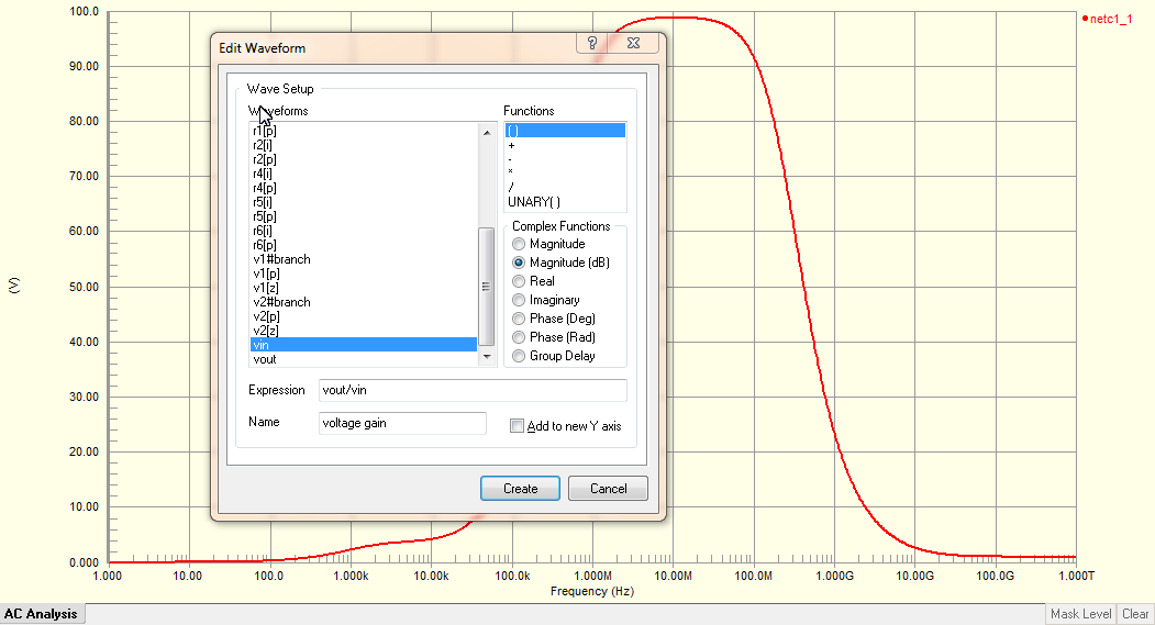
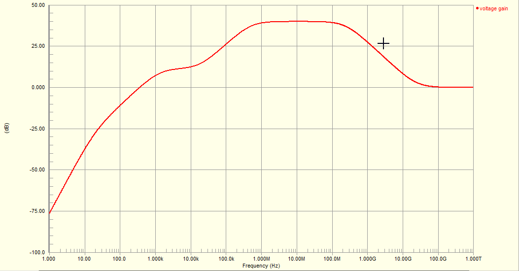
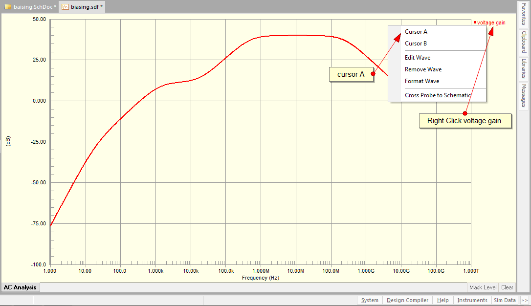
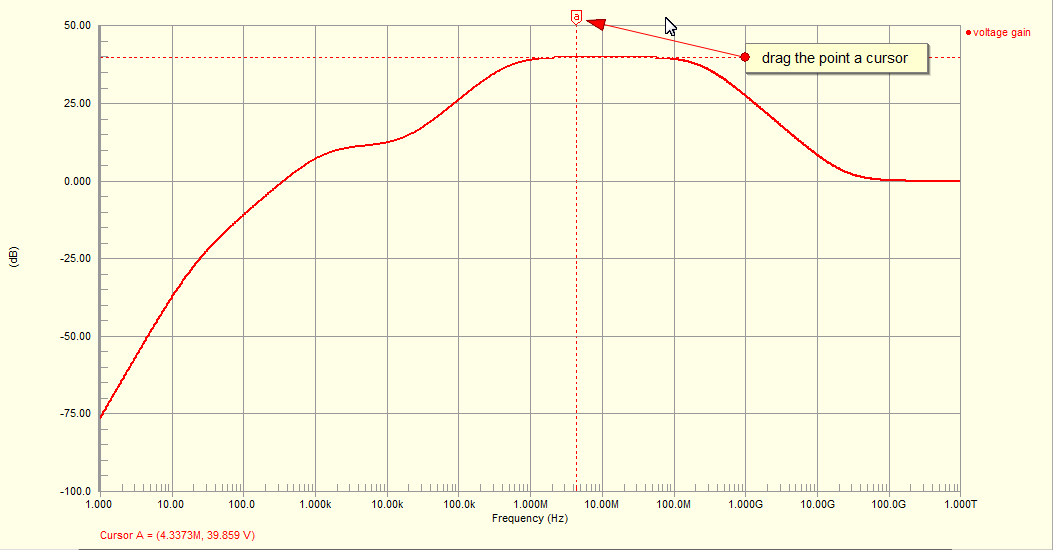
This complete step by step tutorial demonstrates how to design CE amplifier with voltage divider biasing method and simulate the design in Altium Designer. The transistor used is the 2N3904 general purpose transistor.
Suppose we have a signal with amplitude of 10mV(close to actual typical voltage from a microphone) and we want to amplify the signal to give an output signal with some higher voltage amplitude. We begin by assuming the collector current to be 10mA. We also start with a d.c supply of 9V from a battery for example. The first thing we need to do is to bias the transistor in it's linear active region as this is where the transistor will function as an amplifier.
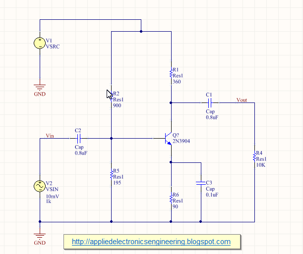
We assume here that you know how to create a new project in altium designer and have a blank schematic open. Once you have the schematic open place the transistor(2N3904), the resistors and a d.c source and connect them as shown in the schematic figure below-
 |
| Fig: Voltage Divider Biasing |
This is the skeleton of the voltage divider biasing. Now change the d.c voltage of the VSRC to 10V. To do this (as some might not know) double click on the VSRC and then click on edit and then select Parameters tab and enter +10V in the value box. This is shown below-
 |
| Fig: Setting up Power Supply |
Click on OK to make the change. To make this value +9V visible on the schematics you have click on the check box and click on edit and again turn on the check box for visible option. This is shown below-
 |
| Fig: Setting up Power Supply |
Also change the designator name to Vcc and after this the source VSRC should look like the one below-
 |
| Fig: Power Supply |
Let's also rename the resistors in the schematics so that the discussion remains intact.
 |
| Fig: Renaming Resistors |
The proper names are now addressed in the above schematic. The resistors R1 and R2 forms the voltage divider resistors.
Now we are ready for the biasing part. At this point you may want to read the
what is transistor baising? post which explains quite a bit what is biasing.
Let's start by making the emitter voltage drop of one tenth of the supply voltage-
\[V_E=\frac{V_{CC}}{10}=\frac{9V}{10}=0.9V\]
Know that the collector current and emitter current are approximately-
\[I_E \approx I_c =10mA\]
We can calculate now the resistor at the emitter-
\[R_E =\frac{V_E}{I_E}=\frac{0.9V}{10mA}=90ohm\]
From this we get the collector resistor value-
\[R_C =4R_E=4*90ohm=360ohm\]
Now we use the below formula to calculate the resistor R1 value-
\[R_1<\frac{\beta_{dc}*R_E}{10}\]
which gives-
\[R_1<\frac{100*90ohm}{10}=900ohm\]
Now to calculate R2 we can use the voltage divider formula-
\[\frac{R_2}{R_1}=\frac{V_2}{V_1}\]
or,
\[R_2=R_1\frac{V_2}{V_1}\]
We have,
\[V_2=V_E+V_{BE}=0.9V+0.7V=1.6V\]
and,
\[V_1=V_{CC}-V_2=9V-1.6V=7.4V\]
Thus using these values we get,
\[R_2=R_1\frac{V_2}{V_1}=900ohm\frac{1.6V}{7.4V}=194.59ohm\approx195ohm\]
The following figure shows the schematics after entering the resistor values-
 |
| Fig: Resistor Values |
Now we add a signal source and a load resistor at the input and output of the circuit.
 |
| Fig: Adding signal source and load |
Double click the VSIN source to edit its properties. Click on edit and then parameters to set the amplitude to 10mV and frequency to 1kHz as shown in figure-
 |
| Fig: Setting up Input Signal |
Similarly change the load resistor value to 10kohm.
 |
| Fig:Setting up Load |
Now we need to add a coupling capacitor between the signal source and the amplifier and another coupling capacitor between the amplifier and the load resistor. Now what is the purpose of the coupling capacitor? Coupling capacitors are capacitors that couples ac signal from the source to the amplifier and blocks dc signal to cross over it. Similarly at the output it allows the ac signal to pass through it and blocks the dc signal. The coupling capacitor also functions to maintain the bias of the amplifier.
Now is the picture where two coupling capacitors at the input and output of the amplifier are added-
 |
| Fig: Adding Coupling Capacitors |
The name of the capacitors have been changed to C1 and C2. C1 is the coupling capacitor at the input and the C2 the coupling capacitor at the output.
How to determine the value of the coupling capacitors? Here is a formula to calculate the capacitance of the coupling capacitors-
\[X_c<\frac{Z}{10}\]
where, Xc is the reactance of the capacitor and Z is the load impedance
We first calculate the value of coupling capacitor capacitance C2 at the output because it will make easier to understand.
\[X_{c2}<\frac{Z}{10}=\frac{R_{load}}{10}=\frac{10kohm}{10}=1kohm\]
Therefore,
\[\frac{1}{2\pi f C_2}<1kohm\]
or
\[C_2>\frac{1}{2\pi f*1k}=\frac{1}{2\pi 1k*1k}=0.159\mu F\]
at f=1kHz
That is at this value C2 is short circuit for a.c signal of 1kHz. But we will take an approximate value of C2 greater than that calculated above as C2= 0.8 uF(assuming 20Hz frequency). This capacitor of 0.8uF can pass any signal above 20Hz including our 1KHz but will block the d.c signal.
Similarly we can just take C1=0.8uF. But if one wishes one can calculate the total impedance after the C1 capacitor (until ground) and use the above formula to calculate capacitive reactance first and then the capacitance. The output impedance for the input coupling capacitor is parallel combination of R1, R2 and the Zin(base) of the transistor.
So taking 0.8uF as our coupling capacitor value we have the following schematic-
 |
| Fig: Adding Coupling Capacitors value |
We also need a bypass capacitor at the parallel to the resistor at the emitter. But how to calculate bypass capacitor value? The value of the bypass capacitor can be determined using the same formula as for the coupling capacitor above. That is-
\[X_c<\frac{Z}{10}\]
The function of the bypass capacitor is to short the ac signal at certain range of frequency to the ground and that is why it is also known as a.c ground. This means here that the a.c signal at the emitter should be grounded at the frequency of interest(1kHz).
Taking f=1kHz, and Z=90ohm gives us decoupling capacitor C3 value of-
\[C_3>17.69\mu F\]
But taking lower frequency into account say as before f=20Hz gives us-
\[C_3>0.088\mu F\]
taking approximate-
\[C_3>0.1\mu F\]
This bypass capacitor with its value is shown in the schematic below-
 |
| Fig: Complete Amplifer Design schematic |
Circuit Simulation Using Altium DesignerBefore we start the simulation we need to attach labels to the wire(or Net) where we want to collect the signal waveform. In this tutorial we will get the waveform of the input signal and the output signal.
To attach a Net label right click on the schematic and choose Place> Net Label or click the Net icon on the toolbar. Add two net labels at the input and output and rename them as Vin and Vout as shown in the figure below-
 |
| Fig: Adding Net Labels |
Compile the project by going to the Project >> Compile PCB Project
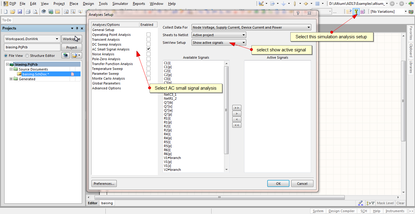
Once this is done, click on the Setup Mixed-Signal Simulation icon on the toolbar as shown in the figure below. If this is not visible you can bring it up and attach that icon to the toolbar by going to the Design>Stimulate>Mixed Sim. This is also shown below-
 |
| Fig: Simulation Setting in Altium Designer |
Now, in order to capture the input and output waveform ensure that the collect data option has voltage node, supply current, device current and power selected. Also set the simview setup option to show active signals.
From the available signal lists select the two signals Vin and Vout and click on the '>' to move them to the active signal list. This is shown below-
 |
| Fig: Simulation Setting in Altium Designer |
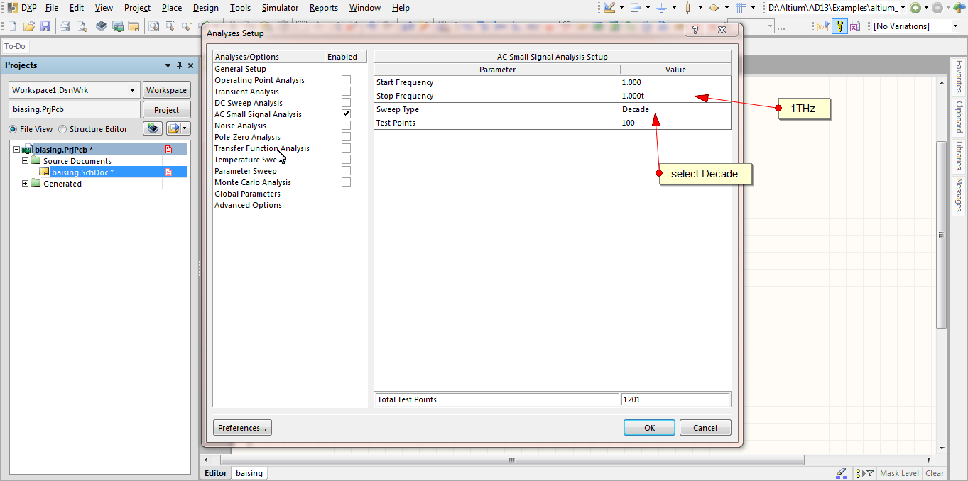
Select the operating point analysis and the transient analysis. To change the default transient settings, uncheck the Use Transient Default. Set the Transient Stop Time to 10m and Transient Step Time to 10u as shown below-
 |
| Fig: Simulation Setting in Altium Designer |
Now to run the simulation, click on the Run Mixed-Signal Simulation as shown-
 |
| Fig: Running Simulation in Altium Designer |
This will generate the desired input(Vin) and output signal(Vout) waveform as shown below-
 |
| Fig: Resulting Input and Output Waveform |
From the waveform we can see that the magnitude of the output waveform is approximately 23mV. Peak to peak voltage of input is ofcourse 20mV whereas the peak to peak voltage of output waveform is 46mV. Notice that the input and output waveform are also out of phase 180 degree. Thus the amplifier designed has produced an output signal that is amplified and inverted.
