Minggu, 30 September 2012

Microcontroller with single LED Project in Proteus

This is a simulation project that shows how to write program in assembly language for PIC16F84A microcontroller that turns on a single LED and use it in Proteus VSM to stimulate the working of the microcontroller controlled LED.

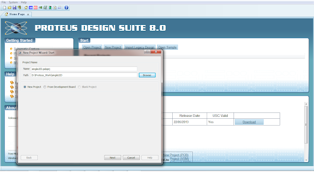
To do this start by creating a new project in Proteus, give some name and save it to some folder.

Microcontroller with single LED Project in Proteus
Click Next. We require a schematic so select Create a schematic from the selected template and choose default or any size you want.

Click Next. We do not require a PCB so select Do not create a PCB layout and click next again.

We do require a Firmware so select Create a Firmware Project and select PIC16 as Family, PIC16F84A as Controller, MPASM(MPLAB) as the Compiler.

Microcontroller with single LED Project in Proteus

Clicking next will bring up the source code editor window and the schematic window. Go to the Schematic and add the following components-
  • 9C04021A3300FLHF3 (330ohm resistor)
  • 9C08052A1002JLHFT (10K ohm resistor)
  • CRYSTAL
  • LED-GREEN
The PIC16F84A micro-controller is already added so no need to add that part.

Microcontroller with single LED Project in Proteus

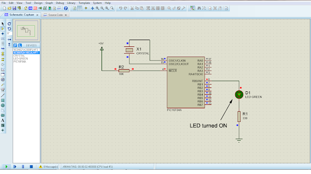
Draw the schematic as shown-

Microcontroller with single LED Project in Proteus

Click on the VCC power and change it to +5V

Now switch over to the Source Code by clicking on the Source Code tab. The Source code editor shows a default template. Delete the template code and Copy the following code below into it.
----------------------------------------------------------------------------------------------------------------------
    processor 16f84A
    include      <p16f84A.inc>
    __config  _XT_OSC & _WDT_OFF & _PWRTE_ON & _CP_OFF

    org    0      ; start at address 0
    goto    main
;=============================
; space for interrupt handler
;=============================
    org        0x04
;=============================
;       main program
;=============================
main:
; Initialize all line in port B for output
    movlw    B'00000000'    ; w = 00000000 binary
    tris    PORTB        ; Set up port B for output
; Turn on line 0 in port B. All others remain off
    movlw    B'00000001'
                    
    movwf    PORTB
; Endless loop intentionally hangs up program
wait:
    goto    wait

        end   
-------------------------------------------------------------------------------------------------------------------------

Code Explanation

The part "processor 16f84A" tells which microcontroller is being used. The "include  <p16f84A.inc>" part is a directive that tell to use the p16f84A microcontroller include file. The __config directive specifies various configuration aspect of the microcontroller such as the type of the oscillator, whether watch dog timer is on or off, whether the Power-Up timer is on or off and code protection is on/off. Then Org 0 tells the assembler to assemble all subsequent code starting at address 0. The next instruction it reads is the main so the program control goes to main. The instruction movlw    B'00000000' tells to load working register with 000000000. The instruction tris    PORTB tells to make the Port B direction as output. Then the sequence of instruction movlw    B'00000001' and movwf PORTB directs to turn on the line 0 of the Port B.

Microcontroller with single LED Project in Proteus
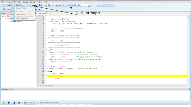
Go to Build>Build Project or click on the Build icon in the toolbar.

Microcontroller with single LED Project in Proteus
If everything is right then the VMS output should show Compiled Successfully as shown-

Microcontroller with single LED Project in Proteus
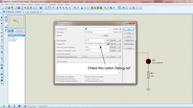
Go back to the Schematic and click on the PIC16F84A to open its properties. Check that the debug.cof is selected as this is the file that will be used for simulation of the microcontroller.

Microcontroller with single LED Project in Proteus

Click OK and go back to the schematic and run the simulation.

Microcontroller with single LED Project in Proteus

Thats it. The LED is now turned on.

For more tutorials visit Proteus Professional Tutorials
Minggu, 23 September 2012

Create Component Faster in Altium Designer

It is really frustrating when one has to spend hours on creating schematic symbols and footprints for parts rather than doing the real design part. It can take hours to build the library and symbol for schematic and footprints. It is especially time consuming to build for component for large number of pins.

This video tutorial shows how designers can use altium designer Smart Grid Tool and IPC Footprint Wizard to quicker build the schematic symbol and footprint and compile them into integrated library.

Here in this video, schematic symbol and footprint for NRF2401A  single chip 2.4GHz transceiver will be build.


For more tutorials visit video tutorial collection and Altium Designer Tutorials

Sabtu, 22 September 2012

How to change Font size in Altium designer PCB

When PCB designs are imported from other PCB design software such as eagle, the top overlay text are much bigger than normal. In such case the text must be re-sized. This short tutorial shows how to resize all the text to suitable size in Altium designer PCB.

Below you can see an example of a PCB design that was imported to Altium designer which has abnormal text size.

change Font size in Altium designer PCB

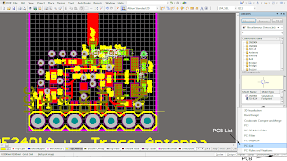
As you can see the yellow colored texts are not readable. To change the size of the text, you can select the PCB tab option at the bottom right corner and then select the PCB List as shown-

change Font size in Altium designer PCB


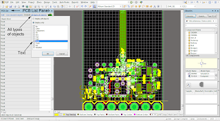
This brings up the PCB List panel. Here we can select all the Text in the PCB and then set text size all at once. To do this, click on the "all types of objects" then select Display only option and then select Text as shown-

change Font size in Altium designer PCB

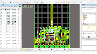
The PCB List will then contain only the Text as object in the list.

change Font size in Altium designer PCB


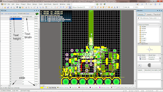
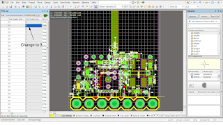
To change the Height and width of the text, navigate to the right side until you see the Text Height and Text Width column as shown-

change Font size in Altium designer PCB


The Text Height is 16mils and the text width is 10mils. We will change the height from 16mils to 10 mils and width from 10 mils to 3 mils. To to this, select the first entry(16) in the Height column, then right click and select the "Select Column(s)" option.

change Font size in Altium designer PCB

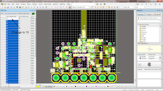
Right click the first entry and select "Edit" and change the number from 16 to 10 as shown-

change Font size in Altium designer PCB

Hit enter to make the change. Now all texts have a height of 10mils.

change Font size in Altium designer PCB
Follow the same steps for the width as for the height to change the width from 10 mils to 3 mils.

change Font size in Altium designer PCB
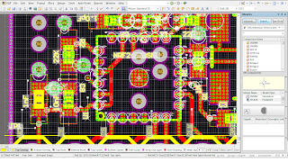
Now if we Zoom in to the PCB we can now clearly understand the yellow overlay text-

change Font size in Altium designer PCB

This completes the tutorial.


Locating components/parts/nets between schematic and PCB

Often during the schematic and PCB layout design and during study of electronic system one requires to know and locate part/wires from schematic in PCB or vice versa. This is especially required in highly dense and complex schematic/pcb work. 

Altium designer has many options available to see and locate components and connection back and forth between the schematic and PCB. One of them is the cross probing tool.

Below shows a typical schematic and its PCB layout-


Now suppose we want to see the oscillator in the PCB. It is quite difficult to locate the oscillator in the PCB because the PCB is simply dense with different components of various sizes filling up the PCB and because of the different color assignment to different layers, pads, silkscreen etc.

Here we will find the cross probing tool in Altium designer very helpful. To do this, go to Tools>Cross Probe from the toolbar as shown.


A + cross will appear at the tip of cursor. Select the oscillator (the part you want to cross probe, in this case oscillator) in the schematic and immediately Altium designer will highlight the oscillator part(footprint) and dim others in the PCB editor-

Now the oscillator is clearly visible in the PCB. To deselect the cross probing tool press ESC key and then select the clear button-


Similarly we can locate parts or nets from the PCB to schematic. Go to Tools>Cross Probe as before or select the cross probe icon and select the part in the PCB to get locate part in the schematic as shown-


Selasa, 18 September 2012

Moving parts between different layers in PCB design

Altium Designer has a very useful feature called the PCB Inspector. Using this PCB inspector one can quickly manipulate and gain insight to different components on the PCB board.

Often times during the component placement phase designer want to look at what various and possible ways there are to place the component(s). In such case the PCB inspector tool of Altium Designer is helpful.

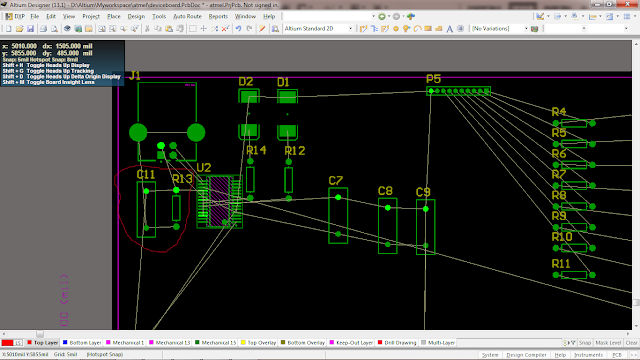
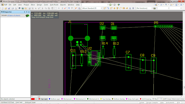
As an example it can be used to move components or parts between different layers and see how the component placement on other layer will have effect on the routing and overall design. To see this, consider the following PCB board with components on it.

pcb design tip using pcb inspector

Notice the capacitor C11 and resistor R13. This is a 2 layer PCB board. Suppose that we want to move these component to the other side and see how the track route and overall design will look like.

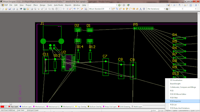
To do this, we select the PCB>PCB Inspector as shown-

pcb design tip using pcb inspector

This will open the PCB Inspector panel-

pcb design tip using pcb inspector

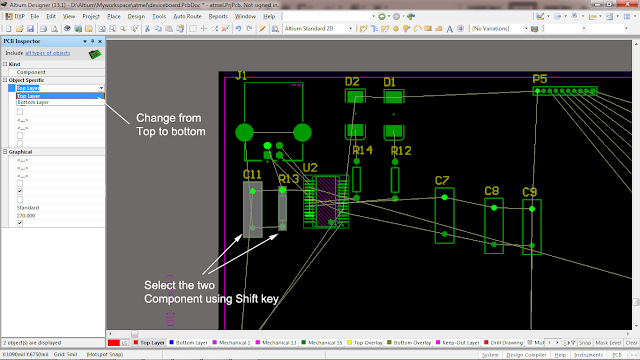
Now select the two components C11 and R13 by holding the shift key and the PCB Inspector will show properties and information of the selected components. Now change the layer from Top to bottom as shown below-

pcb design tip using pcb inspector

Now the component are placed in the bottom layer as shown-

pcb design tip using pcb inspector

Now we can see how while placing the components down in the bottom layers the track routing has changed and the overall look of the design.

For more tutorials visit Altium Designer Tutorials 

Senin, 17 September 2012

Adding 3D step model | Altium Designer tutorial

This tutorial shows how to add 3D PCB step model in Altium Designer.

For more PCB design tutorials visit- Altium Designer Tutorials

Suppose you have a component which has a schematic symbol and footprint but does not have a 3D model. As an example, consider the case where we have the Atmel's ATmega8-16AC which is a 8bit microcontroller. This microcontroller chip has a schematic symbol and footprint as shown-

 
Now if the schematic symbol is double clicked it brings up a new window showing the properties of the component. There under model you can see what other files are attached to it. Here it shows that footprint is available to it but not the 3D model.

Select the footprint and click edit. This will bring up the footprint information. This is shown below-


Now we have attach a 3D model to the footprint. To do so first we require the 3D model for this chip. To get the 3D model we can either make a new one or download an existing one from sites like 3Dcontentcentral.com.

Here we will download the 3D model of this chip from the 3Dcontentcentral.com and attach to the footprint.

To do so, follow the steps.

First go the 3Dcontentcentral.com and download the 3D model step file from the website. For this make a search and you will be shown the available model if the site has one. This is shown below-


Once the component is found, go to the download section, select the Format as STEP(*,step), and version as AP214 as shown in the figure above. Click the download button and download it to a suitable folder in your hard drive.

Now to attach this 3D model step file, we have to open the footprint of the ATmega8-16AC chip and attach the 3D step file there. To find the library that contains the ATmega8-16AC chip make a library search. Here in this case, the footprint and schematic symbol of the ATmega8-16AC chip was inside an integrated library called Atmel Microcontroller 8-Bit AVR. This is shown below-


To get the footprint only, open the integrated library and altium designer will ask whether to extract the integrated library. Select Extract the integrated library. It will be extracted in the same folder containing the integrated library, see above picture.

Once the integrated library is extracted, the schematic library and the PCB library(footprint library) will be visible in the project panel as shown below-


Now select the Atmel Microcontroller 8-Bit AVR.SchLib and then click on the SCH Library tab at the bottom of the project panel and select the ATmega8-16AC. This is shown below-


This is the schematic component/part to which the 3D model will be attached.

Now having noted footprint used for this schematic part, we continue to select its corresponding footprint. To do this go back to the project panel, select the Atmel Microcontroller 8-Bit AVR.PcbLib and click on the PCB Library tab at the bottom of the panel then select the 32A_M footprint from the library as shown-


Now go to 3D view by clicking on key 3 on the keyboard. This brings up the 3D view as shown-


In altium designer, sometimes 3D view will not show. This is because the 3D view is not enabled. In such case then while in the 3D mode, press key "L" and select "Yes" in the Show simple 3D bodies as shown below-


Now go to Place menu and select 3D body as shown-


This bring up a dialog box that allows us to attach the 3D step model (downloaded earlier). In the dialog that appears select the Generic STEP Model, and click on Embed Step Model. Browse to the location and select the step model file that you had downloaded earlier(or the one you want to attach). This process is shown below-


Once the step model is opened the 3D editor window will have the 3D step model added as shown below-

Use the Shift+right mouse button to rotate the 3D models and Ctrl+right mouse button to zoom in/out.


In order to align the two 3D bodies, go to View>Workspace Panels>PCB>PCBLIB Inspector as shown-


Then select the step model 3D body that was added and information about the body will appear in the PCBLIB Inspector panel as shown-


Now we can perform rotation of the 3D body by providing model rotation angle. Here in this case, entering 90 degree rotation angle in the model rotation X will rotate the 3D body as shown-


Depending upon the orientation you should enter the appropriate rotation angle.

To align and have a top view, go to View>Zero Rotation as shown-


Press key 2 to switch to 2D view and to see the center of the component.


Switch back to 3D view and rotate the body upside down as shown-


To align the two component together we need the center of the 3D body(step model). To mark the center of the 3D body (step model) proceed as follows. Select Tool>3D Body Placement>Add Snap Points from Vertices as shown.


Go to the one of the bottom edge of the chip and click once on the edge as shown below-


Now press Spacebar key to enter the midpoint mode. Click then again once on the same vertex and go to the opposite end vertex and click on that vertex.


Now there is a center snap point at the center of the chip.


Switch to 2D view now-


Drag the 2D part of the model with white cross center to the center of the 2D footprint so that their center align as shown-


Switch to 3D view again, the top view is shown below-


The orthogonal top view-


Go to Tool>Remove Snap Points and click on the snap points to remove the snap points.


Double click on the 3D body. This will bring up the extruded 3D body and the step model 3D body information and editing window.


Double click on the extruded 3D option, and standoff height as 0.9mm and standoff height as 0.2mm as shown below-


Double click on the generic step model editor and set the standoff height as 0.6mm as shown-


Now the final 3D model should look like the followings-


Now compile and save the integrated library project in some suitable folder.

Now bring up a new schematic sheet and place the ATMega8-16 component onto the sheet.


Now double click the component and it will bring up its properties window. Select the 32A_M footprint and you can see that the 3D step model has been added as shown below-


This completes the tutorial on adding 3D step model of ATmega8-16 in altium designer.

For more tutorials see Altium Designer Tutorials