Rabu, 29 Agustus 2012

Creating new model in Orcad Capture

In this orcad capture tutorial it will be shown how to create a model library file(.lib) and model symbol file(.olb) for the transistor in Orcad capture which are required for simulation.

Lets say we require 2N3904 transistor in our design work. If we search this transistor we will find it under the library "Transistor" but it has no simulation model and footprint as shown below-


Now we will show how to create a simulation model for transistors like 2N3904 but any component like an IC can be added this way.

1. The first step is to download pspice model for this transistor. The pspice model for components are usually available in the manufacturer website. If the model is not available then another way to create the model is to write the pspice model in a simple text notepad by reading the datasheet of the transistor.

As an example we will show here how to create a pspice model if the pspice is not available in manufacturer website.

The 2N3904 transistor spice model is shown below-

*Model for 2N3904 NPN BJT
.model Q2N3904    NPN(Is=6.734f Xti=3 Eg=1.11 Vaf=74.03 Bf=416.4 Ne=1.259 +Ise=6.734f Ikf=66.78m Xtb=1.5 Br=.7371 Nc=2 Isc=0 Ikr=0 Rc=1 +Cjc=3.638p Mjc=.3085 Vjc=.75 Fc=.5 Cje=4.493p Mje=.2593 Vje=.75
+Tr=239.5n Tf=301.2p Itf=.4 Vtf=4 Xtf=2 Rb=10)

Now copy and paste these text into a notepad and save it with name Q2N3904 (or just 2N3904)and extension .lib, that is as Q2N3904.lib. This file is called the Model Library. Save the file in some location in your computer.

2. Now we have to create the symbol library file for the model library.  To do this open the model editor as shown-


Next select "Pspice A/D" and when model editor opens select "Capture" and click done as shown-


Now go to the File> Model Import Wizard[Capture] as shown-


A new window opens that lets you import the model created earlier. Browse to the location where you previously saved "Q2N3904.lib" file. This is shown below-


Once the Q2N3904 model library (Q2N3904.lib) is imported, the destination location for the corresponding Q2N3904 symbol library will be saved in the same folder(directory) location. So leave the destination symbol library option in default. Click next.

A new window will appear that allows us to associate symbol to the model we are creating. We can choose an existing transistor symbol from the library. In this case, the symbol is matched so we don't need to search for a matching symbol.


Click Finish and the result of this operation will be shown. Notice that there is no error as shown below. Click OK to finish the model creation part.


Now both the model library file(.lib) and model symbol file(.olb) for the transistor is created.


Our transistor model not located in the default Cadence directory. Therefore, to mention the directory for the program to find the newly created model files, go to Pspice>Edit Simulation Profile option. This will bring up a window.
Select the Configuration Files tab and the Libary option on the left side. Click on browse and browse to the directory(folder) where the Q2N3904.olb file is located and select it. Then click on Add as Global or Add to Design. These process is shown in figure below-


Now the transistor is ready to go for simulation. Select the browse button in the Place Part as shown in figure below. Browse to the location of the Q2N3904.olb folder and click open.


The transistor appears in the part window and is ready to be placed onto the schematic. As shown in figure below, the pspice model and footprint icon is also visible now showing that it can be used for simulation and for PCB design.


Now the Q2N3904 transistor can be placed onto the schematic. This completes the Orcad Capture tutorial of creating a new Model required for simulation of parts in Orcad capture.


Sabtu, 25 Agustus 2012

AM circuit design in Altium Designer

In this Altium Designer tutorial an AM circuit schematic will be designed and simulated. The final AM circuit that will be designed is shown below.

AM circuit design with Altium Designer
Fig: AM circuit design with Altium Designer
 Circuit Explanation:

In this simple AM circuit shown, there are two transistors Q1 and Q2 (2N3904). The transistor Q1 is part of oscillator that generates carrier signal while Q2 performs modulation of the input signal shown as sine_signal with the carrier signal from the Q1. The output at the collector of Q2 is the AM signal(in figure labelled AMsignal).

The resistors R2, R4 and R5 are to bias the transistor Q1 and the inductor L1 together with capacitors C7 and C10 forms the tank of the oscillator. C1 is the bypass capacitor. The RF signal at the collector of Q1 drives the modulator or buffer stage Q2. The inductor L2 together with capacitors C6 and C8 forms the tank circuit for the buffer. The AM RF signal appears at the junction of C6 and C8. The resistor R6 is just the arbitrary load resistor.

The output AM waveform is as shown below-
amwaveform
AM waveform
The AM schematic with the battery, input port and the load resistor removed is below-


Now to create the PCB layout for this design, PCB wizard that is available in Alitum Designer will be used. For this goto, System > Files, and then click on PCB Board Wizard from the New from Template.


It then displays an introduction page, clicking next brings up the dimension unit to be used. Here select "metric" because we will be working with mm. This then brings up a list of various standard board layout that can be chosen or you can enter your custom board size.


Minggu, 19 Agustus 2012

Inset Fed Patch Antenna Simulation and Result

This is the third and final part of the Inset Fed Patch Antenna design tutorial using CST Microwave Studio. In this tutorial the designed patch antenna will be simulated to verify it's working.

Readers can visit the first part and second part of the tutorial from the link below-
1st part- Patch antenna design with CST microwave (calculation of dimensions)
2nd part- Design of Microstrip Patch Antenna using CST microwave studio(actual design in CST)


In this part the overall steps in simulation and result of inset patch antenna design tutorial are-
1. Preparation for Simulation
2. Define the output required
3. Running the Simulation and Viewing the Results

1. Preparation for simulation
 Go to Solve menu, then select Frequency, and then define the frequency range from 0GHz to 3GHz as shown below-


We will now add a waveguide port. To do this we have to select the face where the waveguide port will operate. In this case, it is the face of the microstrip feed line where the signal will enter. So we have to select that face. To do this, zoom in so that the signal entry into microstrip face is selected. This is as shown in figure-


After highlighting the port face, go to Solve menu and select "Waveguide Port". A window will open that will be used to set up the port dimension. In this window, set Xmin= Wf/2+5*h, Xmax=Wf/2+5*h, Ymin=h and Ymax=5*h. Leave other setting as default as shown in figure below:


When ok is clicked we have now a Port as shown below-


2. Define the output required
Depending upon the output we wish obtain, we can accordingly perform variety of settings. Here we measure the S11 or Return Loss and view the far field radiation from the antenna. For return loss we do not need to set anything. To view the far field, go to Solve menu and then select Field Monitor. This will bring up a window which allows user to select what the user what to view such as Electric field or magnetic field, power flow, far field etc. Select the Far Field/RCS option by clicking onto its radio button then set the frequency as 2.45GHz and click apply. This step is shown below-


Similarly select the Electric energy density option and click ok to finish up the field monitor settings. When these two are selected as output, it is shown under the field monitor section in the navigation tree. This is shown below-


 3. Running the Simulation and Viewing the Results
After the simulation setting and output requirements are provided, the final step is running the simulation and viewing the result.
Now in order to view the progress of simulation and the simulation progress messages such as warning and error, go to the View menu and tick on the Status Bar and Message Window. This is shown below-


Now, to start the simulation, go to Solve menu and select Time Domain Solver. This brings up the dialog box, select Start to begin simulation, leave other setting as default. This is shown below-


Now to view the S11 or Return Loss of the antenna, go to the 1D Results section in the navigation tree. This will display the S11 or Return Loss of the antenna. To check the minimum value in the plot, right click on the plot and select "Move Marker to Minimum". This gives us the desired result. In this antenna design the Return loss is -20.53dB at 2.457GHz as shown in figure-


Sabtu, 18 Agustus 2012

AM Circuit Design using Proteus

This is a AM circuit design tutorial using Proteus Professional v8. In this tutorial a simple AM circuit will be designed and simulated. The output is a 600KHz range AM signal.

The AM circuit that will be designed is shown below.

Fig 1: AM Circuit
1. Start Proteus and create a new project, give it some name and save it to some folder of your choice. Select Schematic and PCB with no firmware option during the project creation if asked.

2. Turn on the component mode icon and then click the "P" icon to open the Pick Device window which allows you to search component in the proteus library. We will first add the two transistors 2N3904. Type 2N3904 into the search bar as shown and you will be shown the transistor. Now double click the transistor and it will added to the working library.


3. Add the resistor by typing "res" into the search field,  and double click on the item shown in the result window as shown.


4. Add the inductors by typing inductor and select the "B82432C1564K000" inductor or just type "B82432C1564K000" into the search field.


5. Add capacitors by typing cap in the search field and selecting capacitor from the category list and then selecting Generic from the sub-category list. Select two types of capacitors- one  CAP-ELEC which is a generic electrolytic capacitor and the other- CAP-POL which is the Polarized capacitor. This is shown below-

6. Draw the schematic as shown in the Fig 1. The input port, the output port, the ground and the power part in the schematic can be found by clicking the "Terminal Mode". To name the input port and output port, simple double click on them and give them some name. For example here, input port is given "Modulating" and ouput port is given the name "AM_Signal". Also double click on the power supply and enter "+9V" in the input field. This is the 9V battery. This is shown below-


Near the input port we put a sine signal generator with 1V amplitude and frequency of 1KHz. This will act as our audio signal. This is done by clicking on the Generator Mode icon. This brings up an option for number of different signal generator, select the SINE option and put it on the input port wire as shown below-


7. Now to perform simulation and to see graph of the output, click the Graph Mode icon and select the Analogue type. Now near the output port right click, drag and release to get the graph displayed near the output port. Then select the probe icon on the wire and drag it into the graph.


8. To set the simulation time, right click on the top of the graph as shown and select edit properties. There set the start time to 0 and end time to 100m. To start simulation, press the "Space" key on the keyboard. This will start the simulation.


Jumat, 17 Agustus 2012

Design of Microstrip antenna in CST microwave Studio

This is the second part of the Inset fed Patch antenna design tutorial using CST Microwave Studio. In this part of the tutorial, we will use the dimension calculated in the first part to design the patch antenna in CST microwave studio.

Readers can visit the first part or the third part below-
1st part- Patch antenna design with CST microwave (calculation of dimensions)
3rd part- Inset Fed Patch Antenna Simulation and Result
Inset Feed Patch Antenna
fig 1: Inset Feed Patch Antenna

The antenna that will be designed is shown in Fig 1. W and L are the width and length of the patch antenna. The substrate has twice the width and length of the patch antenna, that is, 2W and 2L. The substrate can have other dimension greater than the patch antenna size. In fact here the ground plane underneath the substrate has the same dimension as that of the substrate. There is also a general rule for the dimension of the ground plane but this is not followed here. It is just a dimension which is greater than the patch antenna and the dimension for ground plane has no significant operation on the antenna. Wf and Lf are the dimension of the microstrip line. "d" is the inset fed distance and g is the gap between the patch antenna and the microstrip feed line.
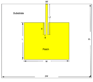
 The dimensions calculated earlier and information obtained from the manufacturer is listed below-

Parameters
Value
Description
W
47mm
Width of Patch
L
39mm
Length of Patch
t
0.07mm
Thickness of Patch(Copper)
h
0.787mm
Height (or thickness) of RT/Duroid 5870 Substrate
Wf
2.3mm
Width of Microstrip feed
Lf
32mm
Length of Microstrip feed
d
12.7mm
Distance of inset fed
g
1mm
Gap between microstrip feed and antenna


1. Create a New Project
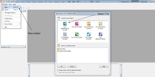
Create a New project by clicking on File>New. On the window that pop-up select "CST Microwave Studio". This is shown in the figure below-
Inset fed Patch antenna design tutorial using CST Microwave Studio
fig 1:
Then a new template window will appear, here select Antenna (Planar). This is shown below-

Inset fed Patch antenna design tutorial using CST Microwave Studio
fig 2:
2. Enter the Parameters and parameter's dimension
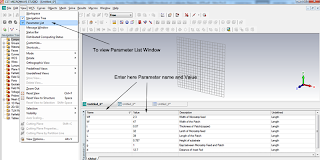
Enter the above mentioned dimensions into parameter table as shown in the figure below-

Inset fed Patch antenna design tutorial using CST Microwave Studio

Note: If the parameter list table is not visible, go to view menu at the top toolbar and tick on the parameter list.

3. Create the Substrate
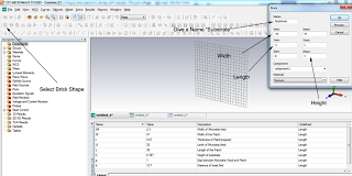
To create the RT Duriod substrate, select the brick shape tool and press ESC. This will bring up a window that allows users to specify the dimension of the substrate. Give a name to the brick shape "Substrate", and enter the Width(-W,W), Length(-L,L) and Height(h) as shown in the figure below.

Inset fed Patch antenna design tutorial using CST Microwave Studio
fig

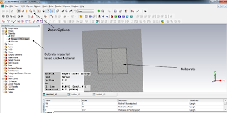
 Once we have the entered the dimension for the substrate, we have to select its material property. For this, go to the drop down menu in the material section and select "Load from Material Library". This will bring up a material library list. Now search for Roger RTDuriod5870 and press "Load" and then "ok" to complete the substrate definition. See figure below.

Inset fed Patch antenna design tutorial using CST Microwave Studio
fig
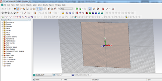
Now, the substrate will appear on the screen. You can Zoom in or Zoom out using the mouse scroll buttom. The front view of substrate created is shown below-

Inset fed Patch antenna design tutorial using CST Microwave Studio
fig

4. Create the Ground Plane
To create the ground plane we have to select the back face of the substrate and define that back face as our ground plane. To select the back face of the substrate either rotate or click on the back view from the toolbar as shown in figure so that back face is visible.

fig
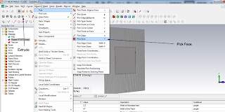
Now go to Objects > Pick > Pick Face or press "f" and double click on the back face. The selected back face will become highlighted. Once the back face is highlighted click go to the WCS menu and select "Aligh WCS with Selected Face". Then again go to Objects > Pick > Pick Face or press "f" and double click on the same back face to select the face.
Inset fed Patch antenna design tutorial using CST Microwave Studio
fig
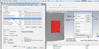
Now select the extrude icon and press ESC key. A new window will pop out that allows users to define the dimension and material of the new surface (that is ground plane). Name the new surface that will be extruded onto the substrate as "Ground Plane", then enter the Height as "t" and in the material section, select "Load from Material Library", and select Copper(annealed) from the material list. Click load and then ok in the subsequent window to finish the ground plane definition.

Inset fed Patch antenna design tutorial using CST Microwave Studio
fig
5. Create the Patch antenna
To create the patch antenna, rotate back to the front face of the substrate. Align the WCS coordinate with the front face by selecting the "Aligh WCS with Selected Face" from the WCS menu and double clicking on the front face. This alignment is shown below-

Inset fed Patch antenna design tutorial using CST Microwave Studio

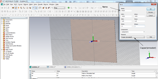
Now select the brick icon on the toolbar and press ESC key for patch antenna. This again brings up the window to enter the dimension and material for the brick. Enter the values Xmin= -L/2, Xmax=L/2, Ymin= -W/2, Ymax= W/2, Zmax= t (Zmin is not required, leave it empty). This is shown below-

Inset fed Patch antenna design tutorial using CST Microwave Studio

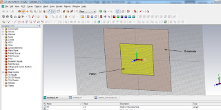
Click "ok" and the patch on substrate will appear as shown below-

Inset fed Patch antenna design tutorial using CST Microwave Studio


6. Create Microstrip Feed Line
To create microstrip feed line, first an empty space will be created and then microstrip line will be added. This makes a gap between the microstrip line and the antenna.
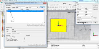
To do this, create another brick for the empty space by clicking on the rectangular brick tool and pressing ESC as in earlier steps. Then enter the dimension value for the empty space as Umin= -(Wf/2+g), Umax= Wf/2+g, Vmin= L/2-d, Vmax=L/2, Wmax= t. Select nickel from the material library as shown, load it and press ok. This process is shown below-

Inset fed Patch antenna design tutorial using CST Microwave Studio

Once this is done a shape intersection window will appear as shown below because the newly created empty space and the patch antenna shape has intersected. Check the "Cut away highlighted shape" radio button to cut away the patch shape and create an empty space. This is shown below-

Inset fed Patch antenna design tutorial using CST Microwave Studio


The patch antenna cut away due to creation of the empty space looks like this-

Inset fed Patch antenna design tutorial using CST Microwave Studio

Now to add the microstrip, create the brick tool again, press ESC key which will bring up the dialog box as before. Enter "Microstrip" as name for the new brick shape, Umin= -Wf/2, Umax=Wf/2, Vmin= L/2-d, Vmax= Lf-L/2-d and Zmax= t. Select copper(annealed) in the material section. This is shown below-

Inset fed Patch antenna design tutorial using CST Microwave Studio

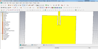
The result is shown below-

Inset fed Patch antenna design tutorial using CST Microwave Studio

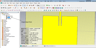
Now, go to the component section of the navigation tree on the left side(from user point of view) as shown in figure and single click on the "Patch" so that it is selected, then click "Add" boolean function on the toolbar,and then single click on the "Microstrip" in the navigation tree to select it and then hit ENTER key on your keyboard. This is illustrated below-

Inset fed Patch antenna design tutorial using CST Microwave Studio

Now the Patch and Microstrip are added together as a single shape as shown in figure below-

Inset fed Patch antenna design tutorial using CST Microwave Studio

The final designed patch antenna  is shown below-

Inset fed Patch antenna design tutorial using CST Microwave Studio

This completes the design step for the inset fed patch antenna.

Next we will simulate and verify the S11 or Return loss at 2.45GHz. See Inset Fed Patch Antenna Simulation and Results