Senin, 06 Februari 2012

Designing Transistor Circuits

Designing Transistor Circuits

Designing a Transistor Circuit is first step in any electronic and electrical circuit design. A Transistor is fundamentally the most essential part in any electronic design. This is because of transistors which makes the electronic system that we see today. Any electronic system capability comes from two things- switching and amplification. This two functions are provided by transistors. For example, in analog systems, amplifiers are needed to amplify voltage, current or Power. A power amplifier driving an antenna at the front end or a power amplifier driving a loudspeakers are examples of application of transistor in analog domain. In digital domain, transistors are used as switches that makes up the various digital gates, NAND, XOR, AND, OR etc.

There are two basic types of widely used transistors- BJT(Bipolar Junction Transistor) and FET(Field Effect Transistor). Each of them have prons and cons. For example, BJT have higher speed response in comparision to FET whereas FET consumes less area than BJTs.

Before designing a transistor circuit, we must know what we want to achieve with the transistor. In order words what is the application or function of the transistor in the circuit. For example, if we want to amplify voice that can be heard on a loudspeaker we can use a transistor as an power amplifier. Here the designing transistor circuit involves, knowing what the input signal(voice) voltage magnitude and frequency are, what power or voltage is required across the loudspeaker. For this it is necessary to know the resistance or impedance of the loudspeaker. Thus the initial assumption would be to know what the input and output characteristics are. Knowing this we can go to the next step for designing the transistor circuit which is selection of the transistors to fit the application. Once the transistor is chosen, the next step is the bias the transistor which is the process of maintaining a constant required output current (the collector current) as much as possible such that the amplification is invariant to temperature changes. Once we know what collector current we require we start by biasing the transistor circuit.

There are many biasing techniques for designing transistor circuits and the most popularly used in the voltage divider biasing. See the post Amplifier Design where details of how to bias a transistor is illustrated.

Circuit Schematic of Transistor Circuit Design

Below shows a schematic drawn in orcad capture in which 2N2222 low power transistor used as an audio amplifier to amplify 0.4V, 1kHz input signal.
Designing Transistor Circuits
Fig: Designing Transistor Circuits

Example of Designing Transistor Circuits

Suppose we have a 8ohm loudspeaker and we require 2V across it to produce 0.5W power. Then below is detailed calculation used in the circuit-

Vcc=IcRc+Vc
IcRc=Vcc-Vc
IcRc=9V-2V
IcRc=7V
Rc=7V/Ic
Rc=7/150mA
Rc=47ohm

Vce at 150mA= 1V
there,
Vce=Vc-Ve
Ve=Vc-Vce
Ve=2V-1V
Ve=1V

Ie=Ic=150mA
therefore,
Re=Ve/Ie
Re=1V/150mA
Re=6.66ohm
R2~6ohm

Vb=Vbe+Ve
Vb=0.6V+1V
Vb=1.6V

R1<100*Re/10
R1<100*6.66/10
R1<66.6ohm
R1~64ohm

Vcc=V1+V2
Vcc=V1+Vb
V1=Vcc-Vb
V1=9V-1.6V
V1=7.4V

R2=R1*V2/V1
R2=65*1.6/7.4
R2=12.97ohm
R2~15ohm

The output signal waveform from simulation for frequency from 20Hz to 1kHz is shown below-

All Frequency waveform at the load
Fig: All Frequency waveform at the load

Minggu, 05 Februari 2012

Class C Power Amplifier Design and Simulation

In this article Class C Power Amplifier circuit is designed stimulate using orcad capture. LC oscillator is designed to oscillate at 25kHz and then input signal frequency and amplitude is varied to get maximum output voltage.

Class C Power Amplifier Schematic

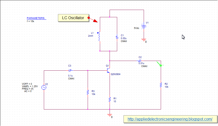
Below is a schematic diagram of a Class C Power Amplifier.

class C power amplifier circuit
Fig: class C power amplifier circuit
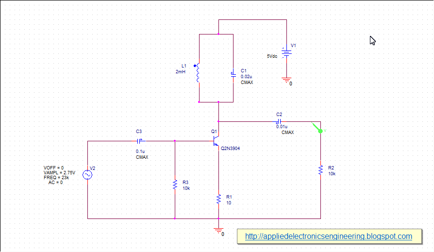
In the above schematic, an input sinusoid signal is applied which has voltage magnitude of 1.25V. The frequency(f) is varied from 15kHz to 30kHz using the parameter sweep tool available in orcad capture. This signal is fed into the class C power amplifier that is made by transistor Q2N3904, L1 and C1 which makes up the LC tuned oscillator. The resistors R3 and R1 are biasing resistors required to bias the transistors(see transistor biasing tutorial). The resistor R2 is a load resistor. The capacitors C3 and C2 are coupling capacitors that blocks dc signals and allows ac signal to pass. This circuit is run by 5V supply.

We know that the frequency of oscillation of the LC oscillator is 25kHz derived from the LC oscillator frequency formula-
\[f=\frac{1}{2\pi\sqrt{LC}}\]
Substituting 2mH for inductor and 0.02microF for capacitor gives 25kHz.

Class C Power Amplifier Simulation

Although we know the frequency of the oscillator we want to know what the frequency of the input signal is at which the magnitude of the output voltage is maximum given that the magnitude of the input signal voltage is 1.25V.  By varying the frequency of the input signal we can get information about the frequency at which the output voltage magnitude is maximum.

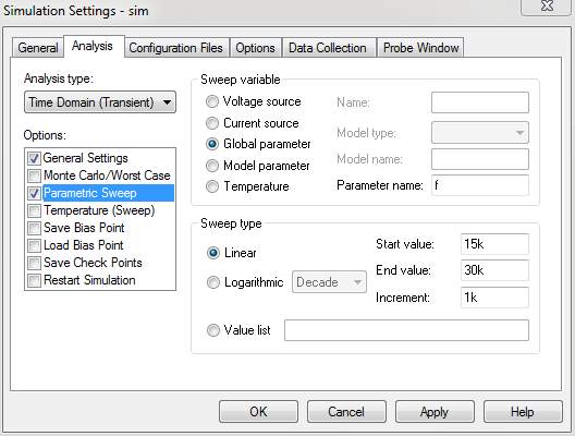
To do this we vary the frequency of the input signal using the parameter sweep tool which is located in the Special library. Then we set up the simulation setting with Transient simulation of run time of 1ms and step size is 10us. Also we set up parameter sweep with f as global parameter, linear sweep type from 15kHz to 30kHz and increment of 1kHz. This simulation setting is shown below-
Simulation setting parametric sweep
Fig: Simulation setting parametric sweep
We put the voltage probe tool at the output as shown in the schematic and run the simulation to get its waveform-
Output Voltage waveforms at different input frequencies
Fig: Output Voltage waveforms at different input frequencies
This waveform shows output voltage waveform for all frequency from 15kHz to 30kHz.

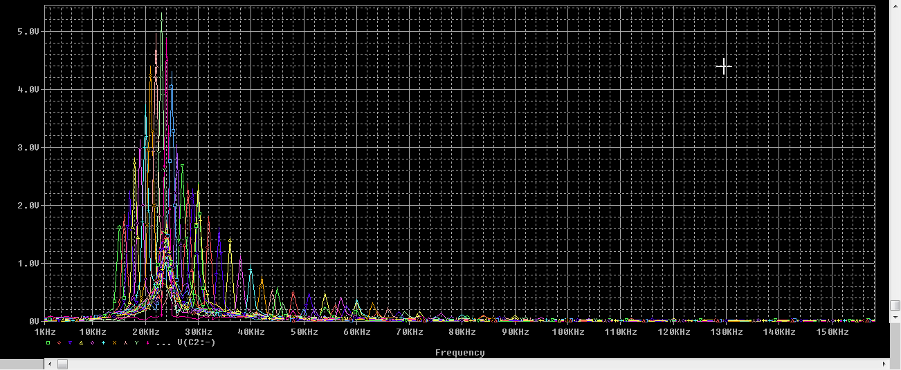
Using the FFT tool available in orcad capture we get the following FT-
Output signal waveform fourier transform
Fig: Output signal waveform Fourier transform

To zoom in we can use the zoom area tool available in the toolbar-
fourier transform of Output signal waveform
Fig: Fourier transform of Output signal waveform
Fourier transform of Output signal waveform
Fig: Fourier transform of Output signal waveform
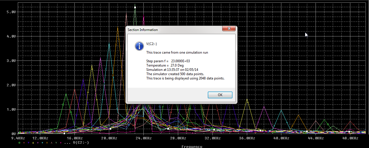
From this final FT graph we can clearly see the frequency at which the magnitude of the output signal is maximum. The green at the center has greatest peak and right clicking on it and selecting Trace Information gives us the its frequency information. This is shown below-
Trace Information from Fourier Transform
Fig: Trace Information from Fourier Transform
This information shows that the frequency of this trace is 23kHz.

We can now change the input signal frequency to this 23kHz.

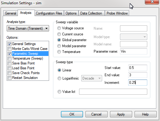
Now we can similarly vary the amplitude of the input signal using the parameter sweep tool. The amplitude is varied from 0.5V to 3V as shown-
Class C Power Amplifier circuit with Voltage Parameter Sweep
Fig: Class C Power Amplifier circuit with Voltage Parameter Sweep
and the voltage variation sweep settings-
Simulation setting for voltage parameter sweep
Fig: Simulation setting for voltage parameter sweep
The output waveform with varying input voltage amplitude is shown below-
Output Voltage waveform with voltage parametric sweep
Fig: Output Voltage waveform with voltage parametric sweep
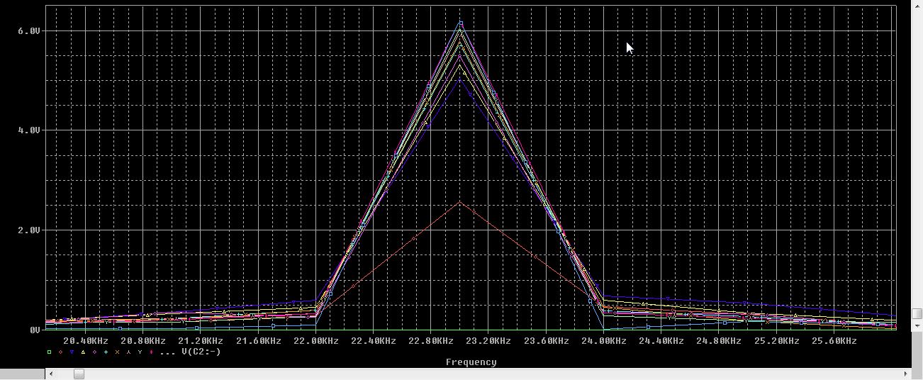
The Fourier Transform is shown below-
Fourier Transform of output voltage
Fig: Fourier Transform of output voltage
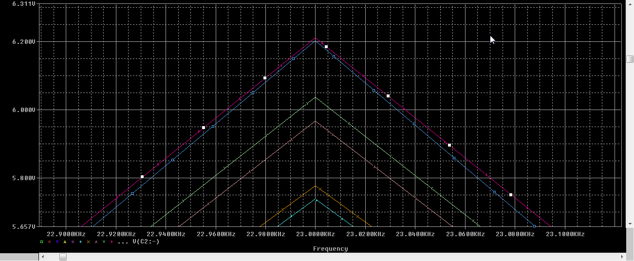
Using the Zoom Area Tool in the toolbar-
Zoomed Fourier Transform of output voltage
Fig: Zoomed Fourier Transform of output voltage
Zoomed Fourier Transform of output voltage
Fig: Zoomed Fourier Transform of output voltage
Zooming into the peak and selecting the peak signal and right clicking to get its trace information gives-
Zoomed Fourier Transform of output voltage
Fig: Zoomed Fourier Transform of output voltage

Output Voltage trace information
Fig: Output Voltage trace information
This shows that the magnitude of the input voltage at which the output voltage is maximum is 2.75V.

Changing the input voltage to 2.75V, removing the parameter sweep tool the final class C amplifier circuit is shown below-
Final Class C Power Amplifier
Fig: Final Class C Power Amplifier

Removing the parameter sweep in the simulation setup and running the final circuit for 2ms gives the following output signal waveform-
Final Output voltage waveform
Fig: Final Output voltage waveform
 And the Fourier Transform gives-
Final Output voltage waveform
Fig: Final Output voltage waveform
This shows that the maximum output voltage is around 6V.

Jumat, 03 Februari 2012

Morse Code Wireless Transmitter

Morse code was one early technique for communication wherein words were sent over copper wires by tapping on a switch that connected and disconnected the wire between transmitter and receiver. The encoding was done such that each alphabets had certain combination of taps. But not only wire but also the Morse code works equally with wireless sound. Below is a schematic of such a system that can send Morse code wirelessly drawn with Proteus Professional 8.

Morse Code Wireless Transmitter
Fig: Morse Code Wireless Transmitter
Powered by a 6V battery and using two transistors(BC558 and BC548) forming a directly coupled amplifier with some resistors and capacitors, and a switch and a loudspeaker the circuit can be used for sending Morse Coded information wirelessly.

The components used are as follows-

Category Quantity References Value Stock Code
Capacitors 1 C1 0.047u Digikey 311-1046-1-ND
Resistors 1 R1 10K Digikey P10KETR-ND
Resistors 1 R2 1.0K Digikey P1.0KVCT-ND
Transistors 1 Q1 BC558
Transistors 1 Q2 BC548
Miscellaneous 1 B1 +6V
Miscellaneous 1 LS1 SPEAKER
Miscellaneous 1 RV1 100K Digikey 3009P-104LF-ND

By the way this BOM was generated by Proteus 8 which is a new feature in Proteus 8.

In the schematic Morse code can be sent by switching on and off the switch. This will set up the signal path and we should hear the sound from the loudspeaker.

Let's check it via simulation. To do this we connect an oscilloscope as shown below-
Simulating Morse Code Wireless Transmitter
Fig: Simulating Morse Code Wireless Transmitter
 And with little Here is a short video clip of the short pulses of morse code-

And here is the screenshot of oscilloscope-

Oscilloscope Output
Fig: Oscilloscope Output
 The settings and the output data obtained from Proteus oscilloscope is also shown below-

Kamis, 02 Februari 2012

class AB Power Amplifier Design and Simulation

Power Amplifiers are essential in the any communication transceivers. They essentially as the name says amplifies the power of the input signal to a desired level at the output stage. The output stage may be a loudspeaker in which case it is called class AB audio amplifier or even an antenna. There are different classes of power amplifiers based basically upon the how much a transistor conducts in a full cycle. For example a class A amplifier is one in which the transistor conducts for full cycle, class B is one in which the amplifier conducts for half a cycle of the input whereas class AB is one in which the amplifier conducts for a cycle between half a cycle and full of a cycle. Here we show a class AB amplifier circuit and simulate it using Altium Designer.

Class AB Amplifier Circuit Schematic

The schematic diagram of a temperature compensated class AB audio amplifier driving load such as loudspeaker is shown below-
Class AB Power Amplifier Circuit Schematic
Fig: Class AB Power Amplifier Circuit Schematic

Circuit Description:
In the circuit above, two complementary transistors 2N3904 which is a NPN transistor and 2N3906 which is a PNP transistor was used. Two diodes 1N4148 are used to prevent damaging the transistors from thermal runaway and to bias the transistors along with the two 3.9Kohm  resistors. Two coupling capacitors(see amplifier design tutorial) are used at the input and output of the class AB amplifying circuit. An input sinusoid signal of 0.5V amplitude and 1KHz is applied to the amplifier and a supply of 20V VDC is applied as shown in the circuit schematic. The 10ohm resistor is the load resistor which is equivalent to a loudspeaker resistance.

Simulation:
The simulation was set up for transient analysis with run time 20ms and step size of 10us(micro second). The input(Vin) and output(Vout) voltage signal was plotted and the result is shown below-

Input Output Signal Waveform of a Class AB Power Amplifier
Fig: Input Output Signal Waveform of a Class AB Power Amplifier

 From the waveform chart above we can see that the input signal peak to peak voltage is 1V whereas the output signal peak to peak voltage is 0.8V.

Similarly the clipped waveform from the upper and the lower transistors for this class AB amplifier is shown below-
Clipped Signals from complimentary transistors of a class AB Power Amplifier
Fig: Clipped Signals from complimentary transistors of a class AB Power Amplifier


Thus the class AB amplifier circuit shown above works as per the simulation.